The invention of the Class AB transconductance
input stage was in response to what had been learned
using by linearizing diodes for the LM13600/LM13700.
The LM13600 really started out just as a practice layout
for a new IC Mask designer. But after the layout
was done, somebody came up with the crazy idea to
turn it into an actual product.
The need was for a practice layout. The LM3080 was being
second sourced. Why not just layout a stereo LM3080?
The linearizing diodes in the LM13700 were thrown in
at the last minute because the 16pin dip package had just
come out, and an extra pin was available. These diodes turned
out to have a few surprises to them which was discovered later.
The linearizing diodes at the time were well suited
to a +/-15V supply world. Signal magnitudes were
often set to several volts. At such levels,
resistors could be used without introducing much
noise, or distortion, or offset.
The problem with the LM3080 was the trade off between
signal to noise and distortion. Applying a larger level
of input voltage will improve the signal to noise ratio,
at the expense of distortion.
While the LM3080 by itself has noticeable distortion,
most customers don't appear to use the linearizing diodes.
The cost of using them being four resistors. Naturally
customers want the distortion to go away for free.
Some other Operational transconductors amplifiers
came out which put the whole pre-distortion circuitry on
chip. The tradeoff here is that the pre-distortion circuitry
needs to run at a fair amount of supply current so as to
not degrade the signal to noise ratio. At that time however,
having low supply current was not an issue.
An alternative method was to use distortion cancellation.
A class AB method similar to what is shown below had
been discovered just after the LM13600/LM13700 came out. But this
idea was not developed since it was a shear miracle that the
LM13600/LM13700 actually became a product. There was obviously
no support from marketing.
Cross-coupled differential amplifier Taiwa Okanobu 4965528
Inventor: Taiwa Okanobu
Assignee: Sony Corporation
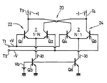
An improvement to the circuit above would be to tie the collectors of
Q2 and Q4 to the supply. This would make the stage operate
in more of a Class AB format, and would improve both the signal
to noise ratio and offset. This is a distortion cancellation technique.
The scale value N is choices to give out the optimum
distortion cancellation.
The challenge was to lower distortion and come as close as
possible to the signal to noise ratio of a two transistor
input stage. Transconductors amplifiers have a headroom problem.
They can usually only put out a maximum amount of output current.
The next step was to find a way to increased the output current
headroom while still using the Class AB techniques.
A Class B stage is a circuit where a essentially the signal path is
off when the input signal is zero. Class B stages have a crossover
distortion problem. A Class AB stage is a circuit where the signal path
is barely on for a zero input signal. This can greatly reduce
both noise and dc offset. But what if the B stage happens to be able
to also take gain? The amount of A biasing can be still adjusted to optimum
distortion cancellation. The circuit above further extends the output
current head room by providing current gain while in the B mode.
With this type of input stage, there are two area scaling ratios.
Ratio N will set how much current gain can be taken in the B mode.
Ratio M adjust
the A bias for optimum distortion cancellation.
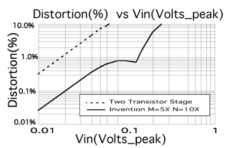
The optimum sizes for M and N appear to be 5x and 10x.
Such ratios appear to push the 1% distortion level to about
a +/-140mV magnitude. A two transistor input stage needs
to have its input signal below +/-18mV to have less than
1% distortion.
^ VC
_____ R3 /_\ R4
| | _/\ /\ /\__|_/\ /\ /\_ _____
| _|_ | \/ \/ \/ \/ | | |
_|_ / _ \IB1 | -> 1.666x IBA1 | _|_ |
\\\ \/ \/ |________ ________| IB2/ _ \ _|_
/\_/\ | | \/ \/ \\\
\___/ |VCN3 | /\_/\
| VBN1 | | VBN2 \___/
^ VC |___________ | VCN4| ___________|
/_\ | QN1 | QN2| | | |QN5 |QN6 |
_|_ | _| _| _| |_ |_ |_ |
/VCC\ |__|'____|'___|' QN3 QN4 `|____`|_____`|_|
\___/ |`-> |`-> |`-> <-'| <-'| <-'|
| 5X | 1X | |10X 10X| |1X |5X
_|_ | | | |_____| |
/// | |____|_____ VEN4 | |
| VEN3 | | |
|_______________/|\________| |
| |________________|
VBP1=0V <- ->
____|' QP1 OUT QP2 `|_
VIN _|_ |`_ _/\ /\ /\_ _ '|_|_
______ / \ _|_ VCN3 _|_ \/ \/ _|_ | ///
|VAC1 |EGin | /// ___ / \ ROUT /// _|_
_|_ _| | ___| GDIF| \\\
/AC1\ | \___/ VCN4 \___/
\___/ |___| _|_
| _|_ \\\
_|_ ///
\\\
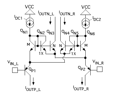
Transistors QP1 and QP2 provide the input to this differential
stage. Assuming no offsets, when to two inputs are at 0V,
transistors QN1,QN2,QN3,QN4,QN5 and QN6 all share the same
emitter base voltage. The current scaling will follow the
area ratios. For instance QN1 will have five times the current
of QN2. Since bias current IB1 is seeing a 6X NPN diode, the
current of QN2 will be 1/6 of IB1. And QN3 will have 10/6 the
current of of IB1.
^ VC
_____ R3 /_\ R4
| | _/\ /\ /\__|_/\ /\ /\_ _____
| _|_ | \/ \/ \/ \/ | | |
_|_ / _ \IB1 | -> 10x IBA1 | _|_ |
\\\ \/ \/ |________ ________| IB2/ _ \ _|_
/\_/\ | | \/ \/ \\\
\___/ |VCN3 | /\_/\
| VBN1 | | VBN2 \___/
^ VC |___________ | VCN4| ___________|
/_\ | QN1 | QN2| | | |QN5 |QN6 |
_|_ | _| _| _| |_ |_ |_ |
/VCC\ |__|'____|'___|' QN3 QN4 `|____`|_____`|_|
\___/ |`-> |`-> |`-> <-'| <-'| <-'|
| 5X | 1X | |10X 10X| |1X |5X
_|_ | | | |_____| |
/// | |____|_____ VEN4 | |
| VEN3 | | |
|_______________/|\________| |
| |________________|
VBP1=+1V <- ->
____|' QP1 OUT QP2 `|_
VIN _|_ |`_ _/\ /\ /\_ _ '|_|_
______ / \ _|_ VCN3 _|_ \/ \/ _|_ | ///
|VAC1 |EGin | /// ___ / \ ROUT /// _|_
_|_ _| | ___| GDIF| \\\
/AC1\ | \___/ VCN4 \___/
\___/ |___| _|_
| _|_ \\\
_|_ ///
\\\
But when Transistor QP1 is turned off, the output current of
QN3 will get much greater. In other words "head room" is being
added to the output magnitude. Now building a differential
input stage using eight transistors instead of two will of course add
both offset and noise. But in the case of transconductance
amplifiers, extending the output swing can have a large effect
on the current mirrors in its following stages.
________________________________________
| VCC | | VCC | _|_
| | | | /VCC\
-> <- -> <- \___/
QP1`|___|'QP2 QP4`|___|'QP5 _|_
_ '| | |`_ _ '| | |`_ ///
| |____|VTA2 | |____|VTA5
| | | |
| <- | <-
|_______|' QP3 _____|_______|' QP6
|VTA1 |`_ | VTA4 |`_
| | | | OUT
| |_____/|\___ |
| | | | R1 1 Ohm
| ______| | |___/\ /\ /\_
_| |_ | VTA6 _| \/ \/ |
__|'QN1 QN2 `|__ |________|'QN5 _|_
_|_ |`-> <-'| _|_ | |`-> ///
/VIN\ | | /// | |
\___/ |__________|VE | ______| VTA7
| _|_ _____ |_ | _|
_|_ / _ \ _|_ _|_ QN3`|__|__|'QN4
/// \/ \/ /VEE\ /// <-'| |`->
/\_/\ \___/ | |
\___/ _|_ _|_ _|_
IBIAS _|_ \ / \ / \ /
\ / V VEE V VEE V
V
Transconductance amplifiers are not like ordinary amplifiers.
Offset and noise cannot be made to be dominated by what happens
at the input stage. A transconductance amplifiers like the
LM3080 has four matched pairs setting its offset and noise.
Say transistor QN1 has a 1mV offset compared to QN2. That means
that about 4% more current flows in QN1 than QN2. At the output, QN5
should see about 4% more current than QP6. But the same thing
would happen if 4% mismatch was applied to QP2, or QN4 , or QP4.
So each matched pair will produce the same amount of output current
error. Since offset and noise both add with power, the offset and
noise of a LM3080 is about the square root of four or twice that of
a simple two transistor differential input stage.
________________________________________
| VCC | | VCC | _|_
| | | | /VCC\
-> <- -> <- \___/
QP1`|___|'QP2 QP4`|___|'QP5 _|_
_ '| | |`_ _ '| | |`_ ///
| |____|VTA2 | |____|VTA5
| | | |
| <- | <-
|_______|' QP3 _____|_______|' QP6
|VTA1 |`_ | VTA4 |`_
| | | | OUT
| |_____/|\___ |
| | | | R1 1 Ohm
VIN=+1V | ______| | |___/\ /\ /\_
_| |_ | VTA6 _| \/ \/ |
__|'QN1 QN2 `|__ |________|'QN5 _|_
_|_ |`-> <-'| _|_ | |`-> ///
/VIN\ | | /// | |
\___/ |__________|VE | ______| VTA7
| _|_ _____ |_ | _|
_|_ / _ \ _|_ _|_ QN3`|__|__|'QN4
/// \/ \/ /VEE\ /// <-'| |`->
/\_/\ \___/ | |
\___/ _|_ _|_ _|_
IBIAS _|_ \ / \ / \ /
\ / V VEE V VEE V
V
But Transconductance amplifiers have a limited output current
swing. So the largest amount of current a LM3080 can put out
is about +/- IBIAS. Suppose IBIAS is set to 1uA. When the
input is zero, the total expected supply current should be about
2uA. And each transistor should be drawing 500nA.
_________________________________________________________________________________
| | | | | VCC | | |
| QP10 | | | VCC | | | _|_
-> <- <- | | | | /VCC\
QP9 `|____|'______|' QP11 -> <- -> <- \___/
_ '| | |`__ |`__ QP3`|___|'QP4 QP6`|___|'QP7 _|_
| | | | _ '| | |`_ _ '| | |`_ ///
|_____| | | | |____|VTA2 | |____|VTA4
_|_ VBIAS | | | | | |
/ _ \ | IBIAS | | <- | <-
\/ \/ | | |_______|' QP5 ______________|_______|' QP8
/\_/\ IBIAS | | |VTA1 |`_ | 1.66 IBIAS VTA3 |`_
\___/ | | | | | | OUT
_|_ __| |__ | |________/|\____________ |
\\\ | | | 1.66 IBIAS | | |
| | | _________| | |
| VBN1 | | | VBN6 | | OUT
|___________ |_/|\________/|\________________ | |
___ | QN1 | QN2| | | |QN5 |QN6 | | |___/\ /\ /\_
_|_ | | _| _| _| |_ |_ |_ | | | \/ \/ |
/// | |__|'____|'___|' QN3 QN4 `|____`|_____`|_| | | _|_
_|_ MX |`-> |`-> |`-> <-'| <-'| <-'| | | ///
/VEE\ | | |NX NX| |1X |MX | VTA5 _|
\___/ | | | |_____| | |________|'QN9
_|_ | |____|______ | | | |`->
\ / | | | | | VT6 |
V |________________/|\________| | | ______|
| | | |_ | _|
VIN=0V <- |________________| QN7`|__|__|'QN8
___|'XQP1 -> <-'| |`->
_|_ |`_ QP2 `|_ | |
/VIN\ | _ '| | _|_ _|_
\___/ _|_ | _|_ \ / \ /
_|_ \ / VEE _| /// V VEE V
/// V \ /
V VEE
But what happens when the input stage is using an AB biased
Transconductance stage that is biased up to draw 2uA supply current?
Well the AB bias technique causes most transistors to draw less
current for a zero input signal. It turns out that transistors
QP3, QP4, QN7, QN8, QP6, and QP7 are are drawing about 3dB
less than 500nA compared to the LM3080. Now there are double the
number of matched transistor pairs. So twice as many transistor
pairs should increase offset and noise by 3dB. However the 3dB
increase in both offset and noise is being applied to a transconductance
amplifier which is being biased at 3dB less current. Some extensive
spice simulations can show that the output noise and offset current
ends up about the same as for a LM3080.
The comparing the AB_Bias Input OTA to a LM3080 Input OTA
AB_BIAS LM3080
1) measure supply current = 2.045uA 2.0uA
2) Measure Max output current = +/- 2.016uA_pk +/- .97uA_pk
3) Measure Max Vin extrapolate = +/- 196mV_pk +/- 51mV_pk
4) Measure Offset_V = +/- 2.7mV_sd +/- 1.6mV_sd
5) Measure Offset_Iout_%Imax = +/- 1.36_% +/- 3.2_%
6) Measure input noise_rtHz = +/- 110nV_rms +/- 56nV_rms
7) Measure 1% THD output current = +/- 1.50uA_pk +/- .334uA_pk
8) Measure 1% THD input V = +/- 146mV_pk +/- 18mV_pk
9) Meaured Rgm = Vin/Iout = 97KOhms 51KOhms
10) Total Output Shot Noise = 159pA_rms 151pA_rms
11) Signal to Noise Clipping = 79.0dB 73dB
12) Signal to Noise 1% THD = 76.4dB 63.5dB
For 2uA of supply current, the output current has twice
the output magnitude because of the extended output
headroom. So for output signals at clipping levels,
there is a factor of two improvement in signal to noise.
At 1% output distortion levels, there is a factor of 4.4x
improvement in signal to noise. And this is all without
drawing any more supply current than a LM3080.
It just so happens that there are other benefits to this input
stage. Today there is the need to operate on a low voltage
single supply. The LM13600 was done in the days when +/-15V
supplies where common. The schematic for the LM324 shown above
describes the automotive market. Amplifiers now needs to
run down to at least 5V, preferably 3V, or as low a voltage as
possible. The LM324 introduced the concept of being able to
run the inputs down to and a little below ground. The usual
requirement is that the inputs can go 200mV below ground.
There is an addition feature if the input stage
is build using lateral PNPs. A trick used for the LM324 and
for that manner the LM741 can be used to protect the inputs.
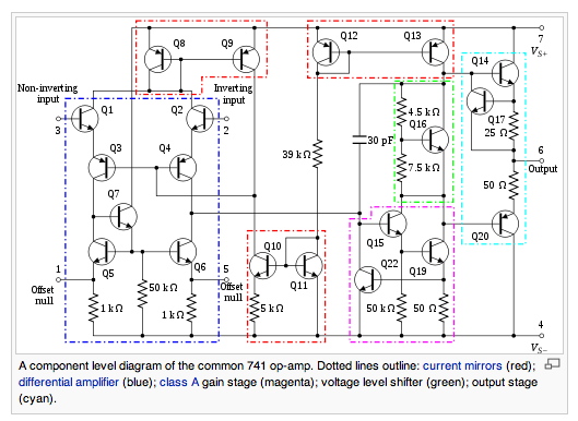
The LM741 was designed in the days when making an Op Amp
fool proof was important. Reverse biasing NPN transistors
to the level of zenering them destroys them. It was discovered
that putting lateral PNP emitters (Q3 and Q4) in series with
NPN emitters (Q1 and Q2) can protect the inputs. Customers
like it when they can connect any input to any supply voltage
without doing any damage.
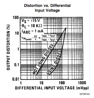
The pre-distortion diodes of the LM13700 really requires the
signal to be at several volts magnitude such that resistors
can resemble current sources. Today the needs are for low
supply voltages, low supply currents, rail to rail output and
inputs if possible. Time change, and so do the requirements.
The following are the features that should now be available.
1)Distortion cancellation.
2)Better than twice the signal to noise ratio
3)Better than twice the signal to dc offset ratio
4)Input protection like a LM741
5)Inputs swing below ground like a LM324
6)Rail to Rail outputs are not too hard.
7)Low supply voltage ( 2 diodes and a sat)
8)Half a LM3080's supply current for the same output
9)Input voltage maximum around +/- 200mV
10)100X the speed if done in BiCmos
There are however some overlooked aspects to using linearizing
diodes. These diodes happen to solve some important
temperature scaling problems. If pre-distortion
stages get replaced by linearized input stages, these
temperature scaling issues still also needs to be taken into
account.
3.11.10_2.35PM
dsauersanjose@aol.com
Don Sauer
http://www.idea2ic.com/