A BRIDGELESS AC<=>DC PFC CONVERTER
12/945,704 filed 11-12-2010
A Rectifier-less Bidirectional AC to DC converter is just a simple
DC to DC being used differently. This invention can
convert AC<->DC
without using any diodes.
The schematic above is showing
diodes
only as a reminder that shoot thru
current needs to be addressed.
The gate driven duty cycle of a
DC to DC converter defines
an output voltage. If this output node instead gets connected
across a secondary of an AC transformer, and if the duty cycle gets
defined to track secondary current, then the secondary will be seeing a
simulated resistor across it. This simulated resistor will absorb
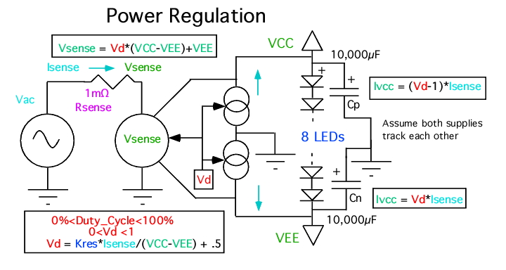
energy and transfer it to the split supplies. It is based on using
the Energy Harvesting Resistor described here.
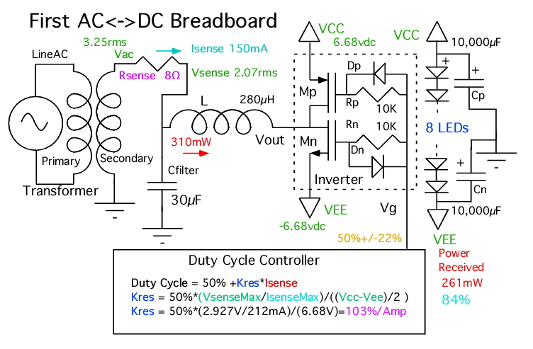
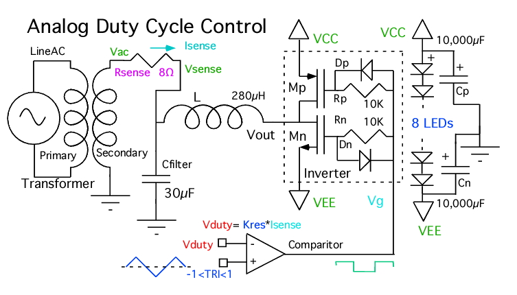
The circuit and equations are shown above. The working breadboard is
shown below.
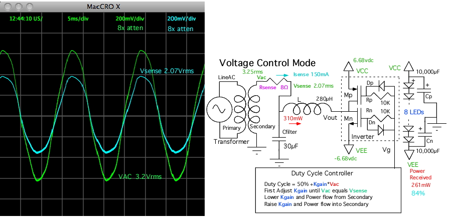
This breadboard takes a 3.2Volt rms 60 Hz input directly off a
secondary of an AC line transformer, and transforms it
directly into +/- 6.7 Volt splits supplies to drive 8 LEDS.
Most of the circuit is for duty cycle modulation experiments.
And this is all being done using analog circuitry.
The full schematic is included at the end. Everything appears
to be working as expected.
There appears to be two main modes of operation. The first
mode is to measure the secondary current, and then use it
to modulate the duty cycle of a simple DC to DC converter
above and below 50%. In the breadboard, this causes the
secondary to think it is seeing a 22 Ohm resistor across it.
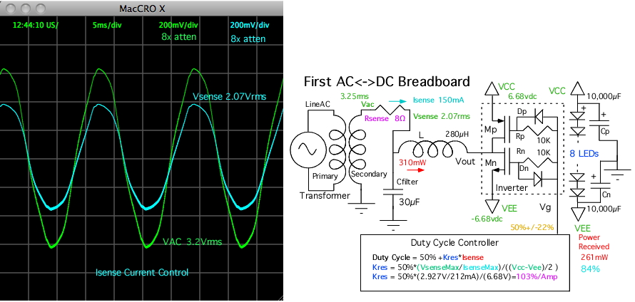
The modulating duty cycle is multiplexing the 150mA rms input
current to the two supplies. The actual AC waveforms of the secondary
voltage Vac and the Vsense voltage are shown above. Both waveforms
are on the same scale. The current flowing across the 8 Ohm
sense resistor is the secondary current.
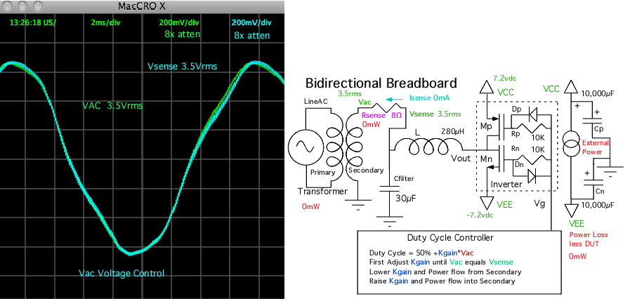
The bidirectional mode of operation involves monitoring the the
secondary's voltage instead. In this case the secondary voltage times
some constant Kgain is used to modulate the duty cycle.
There will be some value for Kgain where the Vsense voltage
equals the VAC input voltage. Under this condition, little power
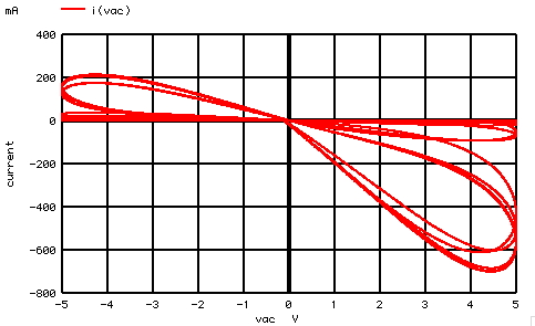
should flow. The two AC waveforms off the breadboard are shown
above. This should raise some questions as to how close can the
duty cycle get to reflect the voltage that will appear at Vsense.
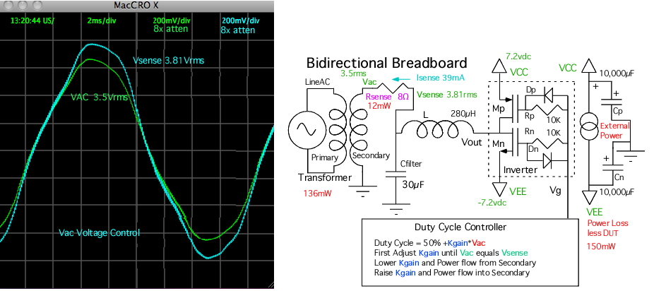
Now if this value for Kgain is increased, then the vsense voltage can get
larger than Vac, and now power is flowing into the 60Hz AC socket. Unlike
normal AC inverters, this is transferring power from the split supplies
as a negative resistor. The waveforms above show that Vsense is larger
than Vac. An external power source needs to be applied to VCC and VEE
to do this test. It appears that the power drain on the external supply
is what would be expected.
Lower the value of Kgain enough, and now the power is flowing from AC to DC.
This method of voltage driving the duty cycle mode appears to be
ideal for bidirectional AC<->DC power transfer since the circuit goes to an
open circuit between the power flow directions.
In this breadboard, the efficiency appears to be around 84%.
It is not obvious how this invention is little more that just using
a simple DC to DC converter in a new application. If that is so,
then the same efficiencies for DC to DC converters should be possible.
This breadboard is actually self starting. When the AC first turns
on, it forward biases the drain bulk junctions of both
power MOSFETs. This turns on the duty cycle controller which
drives the split supplies to a level higher than the AC input
voltage.
When the breadboard is doing the job of a full wave rectifier,
it loads the AC line exactly like a resistor. According
to some recent articles in EDN and Power Electronics Technology,
things like having a high power factor is becoming important.
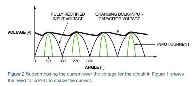
Apparently the nonlinear loading of full wave rectifier circuits
is starting to create a need to raise the power factor
of AC to DC convertors.
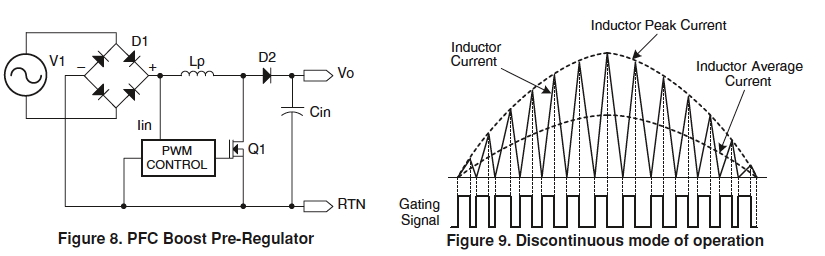
The figures above are from a Fairchild application Note about Power factor
correction. The attempt is to be able to draw power off the ac
line like a resistor. Not very many power factor reduction
methods however lack rectifiers in the power signal path.
The breadboard sure does look like it can load the ac line like a
linear resistor. And even as a negative linear resistor. If solar power
becomes more widespread, would it generate a need for a high power factor
DC to AC convertor?
The power companies are installing smart meters in peoples homes.
This might allow power companies to charge customers at different
rates over the day. Could it be economical someday to store AC power
into home batteries during the time when rates are low, and then
reconvert it back to AC for use when rates are high?
The invention is mainly just a DC to DC converter with differences
in terms of input/output ports, and in how the duty cycle gets
defined. The easy way to do the duty cycle in analog is to build
up a triangle waveform, and stick it into one input of a voltage
comparator. An analog signal voltage on the other input will modulate the
duty cycle.
The analog signal and its effect on the duty cycle is doing two things.
First it generates a voltage at Vsense which is scaled between the two
supply voltages. Second, the duty cycle multiplexes any current through
the sense resistor between the two power MOSFETs and their power supplies.
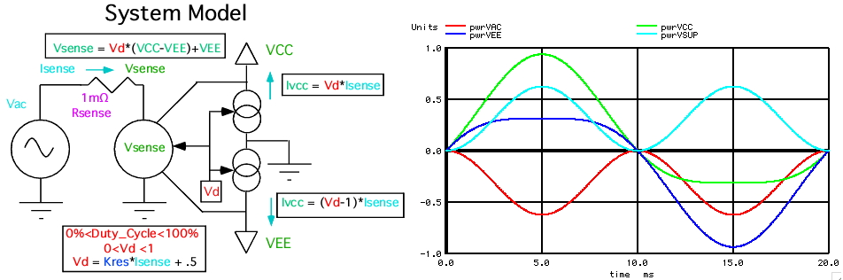
The system model above can show all the equations. For this system model,
the analog voltage Vd is being defined to go from 0 to 1, which
corresponds to a 0 to 100% duty cycle. This duty cycle Vd is being modulated
by the Isense current at some gain. The Vd voltage will both define the
voltage Vsense, and will multiplex any Isense current. Consider what happens
when Vac and Vsense are identical. No Isense current will flow, and zero
current will get multiplexed between the two MOSFETs.
Because the Vd term, which defines the Vsense voltage, is being scale
by the input current, the Vac voltage source will see a load looking
like a linear resistor. Now the current multiplexing will always be charging
up one of the supplies and discharging the other. But when the total
power of both supplies are summed together, they are receiving
close to the same power that the Vac source is being loaded with. Naturally
any IR drop in the power path will reduce efficiency.
This invention tends to have a native output format of power
regulation. For instance, if the output loads are LEDs,
and if the voltage across LEDs can drift with temperature,
the output current will auto-adjust itself the maintain the same output
power.
For the sake of tying up any loose ends, one might be
inclined to make the Vd value track the inverse of the supply
voltages. Since the Vsense voltage is being scaled by the
supply voltages, that means the Vsense magnitude should be
insensitive to the supply voltages. If so, then the same input
Isense produces the same Vsense. So the simulated load resistance
across Vac will not change. So the power transfer will be independent
of the split supplies voltages.
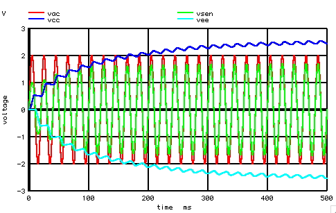
Suppose both VEE and VCC increase by 10%. The same Isense current
should produce a Vd with a 10% decrease in modulation. But the
Vsense is also scaled by the 10% higher VCC and VEE voltages. So Vsense
comes out the same. But the multiplexing of Isense current has
been reduced by 10%. So the two supplies are at a 10% higher voltage,
but they are receiving 10% less charging up current.
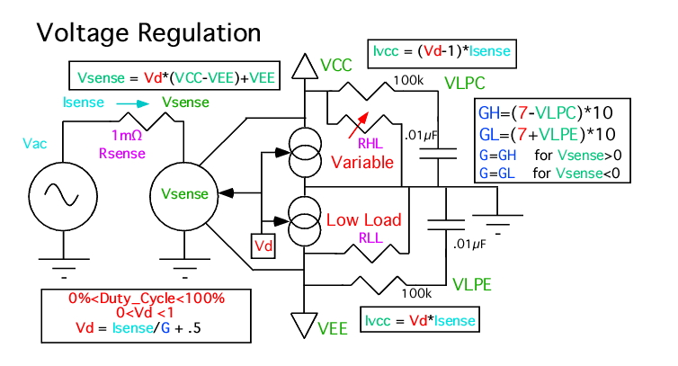
Now normally the output power is formated in a voltage regulated
mode. There is nothing stopping the voltage to current relationship
to the input resistor from being adjusted in terms of both magnitude
or asymmetry. Because VCC gets charged up when Vac is positive, and
VEE when negative, it is possible to regulate both VCC and VEE
independently. The system simulation above shows both VCC and VEE
being regulated to 7 volts. The supply voltages are low pass
filtered since feedback should have a one pole compensation.
The loop gain is set to 10. Different values for G get switched
in depending on Vac
polarity.
In this example, VEE will lightly load with constant 50uA load.
But VCC will vary its load in steps over three orders of magnitude.
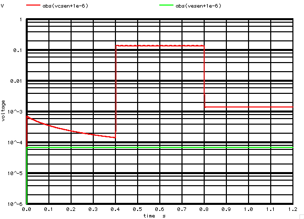
Under heavy load, one would expect VCC to develop some ripple.
But VEE appears to develop ripple at the same time. This is
due to the fact that whenever VCC is being charged, VEE is
being discharged. The VEE feedback loop needs to recover this
lost charge when Vac is negative. So even when VCC is
the only supply being used, the Vac voltage can not be completely
asymmetrically loaded.
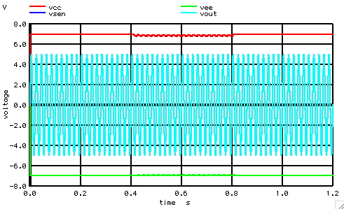
The asymmetry of the current loading on the AC line is shown
above. So this type of AC to DC converter cannot load the
AC line like a one diode rectifier. The lowpass filtering
is not at the moment low enough to reduce the looping in the current loading
curve. These low pass filters will affect the voltage regulation
response to load current spikes. The step response to a high load
current appears to be fast attack, slow decay.
For single supply
applications, it may make more sense to build up
a second DC switching network as is shown on figure 9 on this web page
to transfer charge from one supply to the
next. This enables the resistive
loading to be symmetrical.
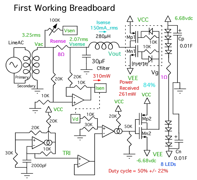
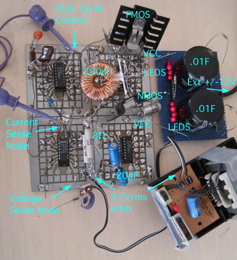
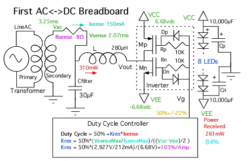
The full circuit for the breadboard is above. A secondary
sense current node and secondary voltage sense node are
provided, and both have been checked out. A LM13600 is being used
to provide an easily scaleable triangle wave, and it is also
used as a voltage comparator. A LM6144 is being used to buffer the
triangle wave, and to measure the current through the 8 Ohm sense resistor.
A CD4007 is being used to drive the Power MOSFETS. These MOSFETs have
large capacitances, and adding some diodes and resistors appear to
reduce the shoot through current.
Most of the supply current is going to the LM13600. It draws in fact
a little too much supply current. It is mainly being used just
to check out some scaling concepts. The duty cycle controller
mainly needs just a triangle wave source and a comparator.
The gate resistor/diodes networks certainly could be replaced with
something better in order to operate at higher frequencies. The
sense resistor is set at 8 ohms in order to make the voltage across it
obvious enough to show things like bidirectional power flow.
The Triangle wave is running below 20KHz, so the 30uF cap
(two 60uF electrolytics) is chosen just to make the
Vsense signal look clean.
Other breadboard experiments are in the works. Running spice simulations
side by side with a working breadboard has some crosschecking advantages.
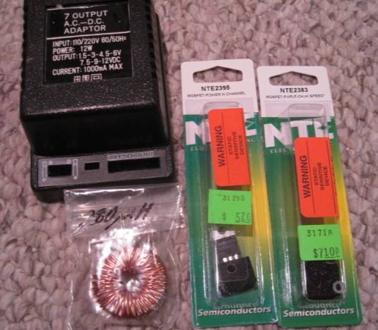
Some of the components used to build the AC<->DC converter hardware are
shown below. For
the moment, the breadboard is mainly being used for
proof of concept.
There appears to be a lot of recent patent activity in
the area
of building "bridgeless PFC convertors". The following are
some of the patents.
11_584_983_Method_and_apparatus_for_high_efficieny_rectifier
11_204_307_AC_to_DC_power_supply_with_PF
11_302_544_Simple_partial_switching_power_factor_correction
11_474_712_BRIDGELESS_BI_DIRECTIONAL_FORWARD_TYPE_CONVERTER
11_480_004_High_efficiency_power_converter_system
11_706_645_AC_to_DC_voltage_converter_as_power_supply
12_401_983_BRIDGELESS_PFC_CIRCUIT_FOR_CRM
12_798_682_Bridgeless_PFC_converter
3295043_MASSEY_D_C__TO_D_C__REGULATED_CONVERTER
4183079_DC_AC_inverter
4523266_AC_to_DC_conversion_system
4943902_AC_to_DC_power_converter_and_method
5570276_Switching_converter_with_open_loop_input_regulation
5815380_Switching_converter_with_open_loop_Primary_regulation
5815384_Transformer_uses_bi_directional_synch_Rectifiers
6115267_AC_DC_converter_with_no_input_rectifiers
6157182_DC_DC_converter_with_multiple_operating_modes
6608522_DC_to_DC_converter_providing_stable_operation
7250742_Digital_control_of_bridgeless_power_factor_correction
7265591_CMOS_driver_with_minimum_shoot_through
And here is some more
information for those who may be interested.
A
BIDIRECTIONAL PWM THREE-PHASE STEP-DOWN RECTIFIER
A
bidirectional, sinusoidal, high-frequency inverter
A
DUAL INPUT BIDIRECTIONAL POWER CONVERTER
A
new structure for bidirectional Power flow
BI-DIRECTIONAL
INVERTER-CHARGER
Bi-directional
single-phase half-bridge rectifier for power quality
BiDirectional
Converter
Bidirectional_UP_Inverter
Synthesis
of Input-Rectifierless AC/DC
11.28.10_10.11AM
dsauersanjose@aol.com
Don Sauer
http://www.idea2ic.com/