TAPE_OUT_4_FREE
(just add time and skill)
The following is mainly a visual cheat sheet on how to use
"iceditor'. The another Template file found else where on this
site
shows some other how-to details A bandgap with a CMOS inverter is used
here as an example to go from a Spice netlist, on
to a layout, then on to design rule checking (drc), then onto geometry
extraction, then on to layout vs schematic (LVS),
and lastly on to generating a GDSII stream file. Every file used
for all stages in this example is included in this one web page.
A lot of critical steps and details are required to convert a schematic
to a finished GDSII file. But hyperlinking can also capture
all the interrelationships. This web page organizes the big picture of
a full IC layout process in the order at which each stage
is performed . Hyperlinking allows quick navigation from any stage in
the big picture down to any critical detail at the smallest level.
The smallest details are usually what make the difference between
something working or not. But the big picture always needs to
be watched in order for all critical details to be completely
compatible with all the other critical details.
The ability to easily navigate between a macro view and micro view in a
web page has great potential. The following are
the manuals that come with "iceditor".
Navigating to critical details can become time consuming and
frustrating when using just these manuals. The problems usually
are simple, but finding out what to do about them is much more straight
forwardwhen
using a cheat sheet.
...Don Sauer 10/17/09
dsauersanjose@aol.com
=========DOWNLOAD_AND_INSTALL_ICED=======ClassicICEDInstall.exe========= Goto the following site
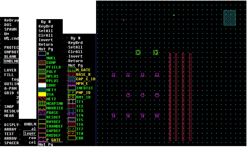
Any Process has if own set of layer definitions and ways to
recognize
the various geometry's.
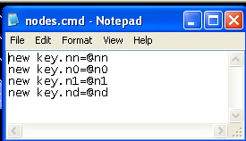
A new LAYER
file defined the layer names,numbers, colors and calma numbers.
A new Design
Rule Check file
defines minimum and maximum spacing between all the layers.
A new EXTraction
file defines how to recognize all the geometry's from the layout.
The new LVS
file is a control file that sets the options on how to run the Layout Versus Schematic
checking program.
Working examples of these files are linked below.
First comes design which involves testing a schematic in a SPICE
simulation.
The SPICE simulator reads in the schematic as a NETLIST
and the LVS program can do the same.
.SUBCKT
TOPCELL VCC VEE
VBG IN OUT QP1
NBASE PBASE VCC
L_PNP 1 QP2
PBASE PBASE VCC
L_PNP 1 QN1
NBASE NBASE NE
V_NPN 1 QN2
PBASE NBASE VBG
V_NPN 10 RB1
VBG
NE
61k RB2
NE
VEE
180k MP1
OUT IN
VCC VCC PMOS W=1U
L=1U MN1
OUT IN
VEE VEE NMOS W=1U
L=1U C1
OUT
VEE
1P .ENDs A schematic is of course is needed to do
the layout. * *
^ *
VCC /_\ *
____________________| *
|
| *
-> PBASE <- *
QP1
`|___________|'QP2
^ *
_ '| |
|`_
VCC /_\ *
|
|
|
| *
|
|______|
<- *
|
|
___||MP1 *
|
|
| ||_
___ *
|_____
|
___ | |_________|OUT| *
|
|
| |IN
|_| | |
|___| *
|_ | NBASE _|
QN2 |___| |
_| _|_ * QN1
`|__|_________|'
10X
|__||MN1 ___ C1 *
<-'|
|`->
||-> _|_ *
|
|
___
_|_ \\\ * NE
|____________/\
__|__|VBG|
\\\ *
| 60K
\/ |___| *
|__/\ ____ RB1 *
\/ RB2| *
180k _|_ *
/// VEE
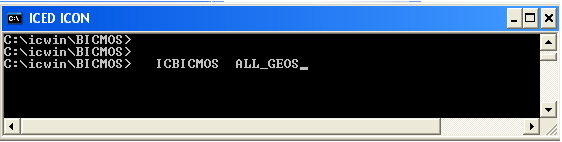
The layout window is opened by calling out the StartUp_batch_File
and then a name of a "Cell".
If the Cell of that name does not exist in the directory, a new Cell
with that name is created.
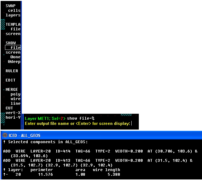
ICBICMOSALL_GEOS
The easiest way to do a layout is to have Mimimum_Geometry_Cells for
all the transistors or resistors or capacitors
already laid out such the all the cells can be manually placed next to
each other and be DRC clean.
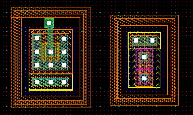
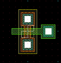
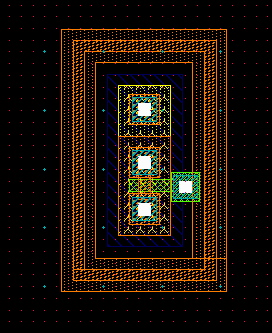
For example the cells for a NPN and a PNP are shown separately
below. These cell file mainly consist of
data points corresponding to rectangles. The file contents are shownhere and here.
These cells are designed so when the external isolation rings over lap,
the spacings are automatically DRC clean.
Variable Geometry's like resistors will need to be stepped in first as
a template cell.
Then the Resistor can be ungrouped and resized as needed. The
program will resize some
of the resistor's geometries which can be viewed here.
CMOS geometries often need to be resized too. It is common
practice to make geometries
such as NMOS
and PMOS
use the Poly defines the transistor size. A fast way
to start layout is to first layout all geometries to their intended
size. Knowing what size
things are helps in showing how things want to group together.
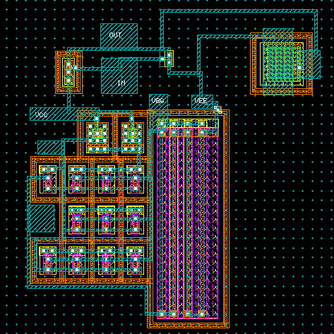
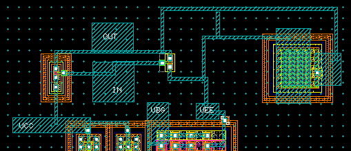
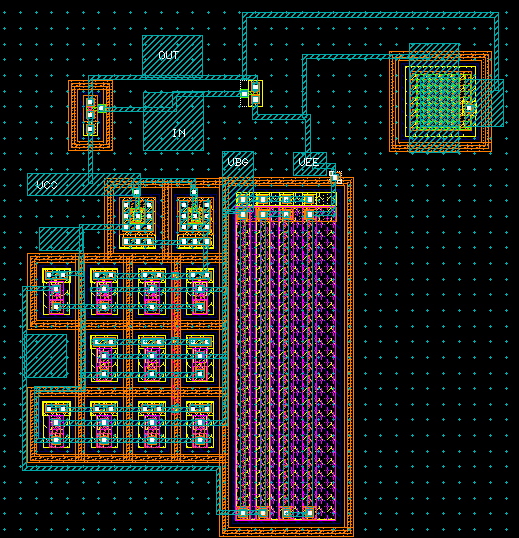
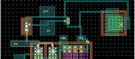
Layout of an IC is very much like drawing a schematic, except layout
cells replace schematic symbols.
In fact, layout is much like making a breadboard. First you collect all
the components. Then you
see how things want to be arranged. Make all all the geometries such
that when they butt up against each
other, the spacing is all correct. Label all the components to match
the schematic. Now just hook up
same as before, but use the metal layers in the layout.
Common Documentation in both the layout
and the schematic/netlist can be a real time saver.
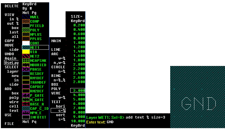
To Label a Metal1 Node "GND" , select the layer and then add text.
The Whole Layout
will include some features such as cells and wires.
Labeling everything like the schematic
can really save time. The layout
is often
very similar to the schematic as is shown below *
^ *
VCC /_\ *
____________________| *
|
| *
-> PBASE <- *
QP1
`|___________|'QP2
^ *
_ '| |
|`_
VCC /_\ *
|
|
|
| *
|
|______|
<- *
|
|
___||MP1 *
|
|
| ||_
___ *
|_____
|
___ | |_________|OUT| *
|
|
| |IN
|_| | |
|___| *
|_ | NBASE _|
QN2 |___| |
_| _|_ * QN1
`|__|_________|'
10X
|__||MN1 ___ C1 *
<-'|
|`->
||-> _|_ *
|
|
___
_|_ \\\ * NE
|____________/\
__|__|VBG|
\\\ *
| 60K
\/ |___| *
|__/\ ____ RB1 *
\/ RB2| *
180k _|_ *
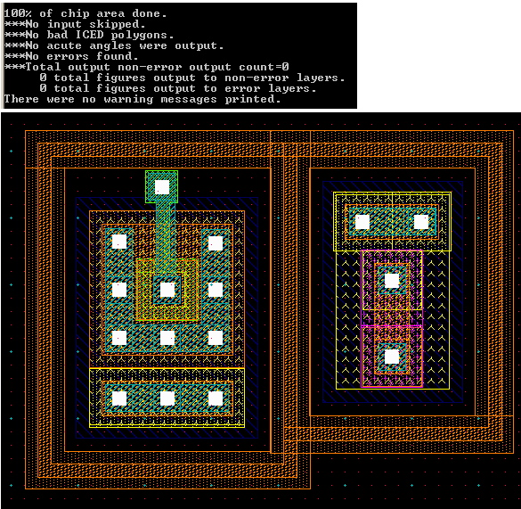
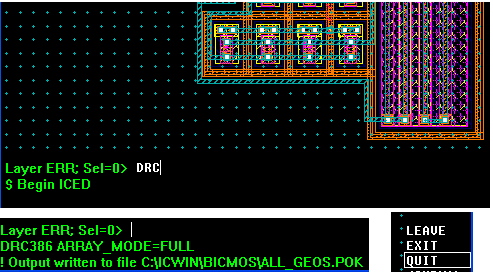
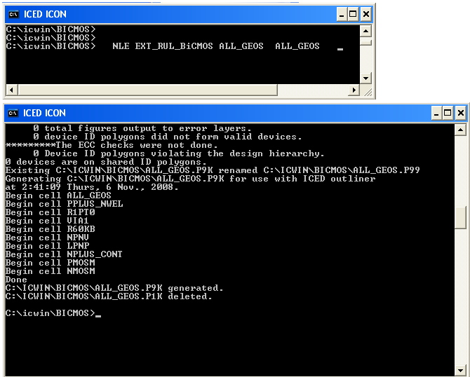
/// VEE =========CREATE_A_POK_FILE=======c:\icwin\BICMOS\ALL_GEOS.POK============
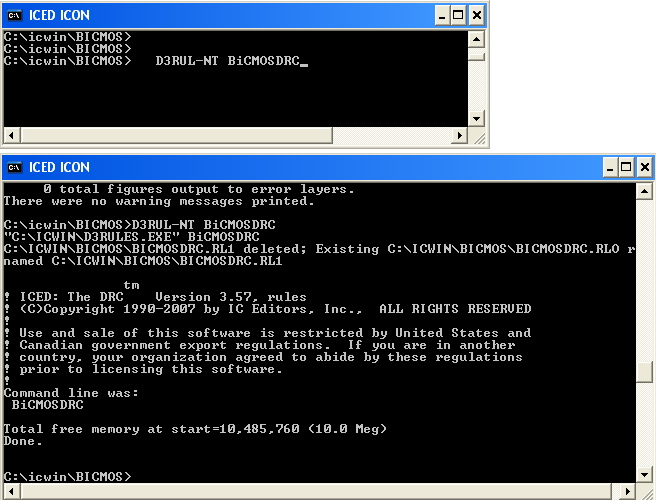
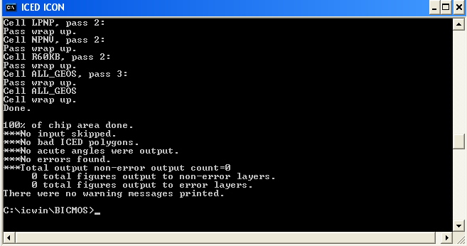
A binary POK cells need to be created of the finished layout.
This is done by just typing DRC into the layout window.
MOS transistors and Capacitors appear to allow for scaling between the
layout and the schematic.
But bipolar transistors don't appear to allow for this
scaling. A perl program can fill in for now.
SCHEMATIC
|
LAYOUT
|
|
#
:1
| #
:1
MN1
|
274
X
:0
Y
:0
| X
:10
Y :79
MODEL
:NMOS TYPE
:NMOS | MODEL
:NMOS TYPE
:NMOS LENGTH
:1 WIDTH
:1 | LENGTH
:1 WIDTH
:1
|
#
:2
| #
:2
MP1
|
821
X
:0
Y
:0
| X
:-42
Y :74
MODEL
:PMOS TYPE
:PMOS | MODEL
:PMOS TYPE
:PMOS LENGTH
:1 WIDTH
:1 | LENGTH
:1 WIDTH
:1
|
---------------------------**
PARAMETER ERROR **--------------------------- #
:3
| #
:3
QN1
|
280
X
:0
Y
:0
| X
:-53
Y :16
MODEL
:V_NPN TYPE
:NPN | MODEL
:V_NPN TYPE
:NPN AREA
:1
| AREA :9.1
|
---------------------------**
PARAMETER ERROR **--------------------------- #
:4
| #
:4
QN2
|
836[M,10]
X
:0
Y
:0
| X
:-53
Y :-26 MODEL
:V_NPN TYPE
:NPN | MODEL
:V_NPN TYPE
:NPN AREA
:10
| AREA :91
|
---------------------------**
PARAMETER ERROR **--------------------------- #
:5
| #
:5
QP1
|
59
X
:0
Y
:0
| X
:-27
Y :40
MODEL
:L_PNP TYPE
:PNP | MODEL
:L_PNP TYPE
:PNP AREA
:1
| AREA :6.76
|
The layout program does not automatically load in calma
numbers. They have to be loaded in from the menu.
The normal layer
file needs to be loaded again.
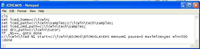
=========CREATE_A_NEW_STARTUP_FILE=======c:\icwin\ICBICMOS.bat========= cls set iced_home=c:\icwin; set
iced_path=c:\icwin\samples;c:\icwin\tech\samples; set
iced_cmd_path=c:\icwin\tech\samples; set drc_path=c:\icwin\tutor; if _%1==_ goto done c:\icwin\iced
%1 start=c:\icwin\BICMOS\BiCMOSLAYERS
menu=m1 pause=0 maximize=yes win=500 :done
=========NEED_A_NEW_LAYER_FILE=======c:\icwin\BICMOS\BiCMOSLAYERS.cmd============ VIEW OFF $ MENU
"M1";
KEEP_LIBRARY_CELLS=ASK; DISPLAY CELL_DEPTH=100; PATTERN
"SAMPLE";
FILL MIXED ON AUTOPAN
ON
PIXELS=100
SECONDS=0.5;
ARROW MODE=EDIT DISPLAY
CELL_LABELS=ON
OUTLINE_DEPTH=1
EDIT_STACK=OFF CURSOR
1 SNAP=ON SPACER
OFF
SPACE=0.0
TRACK_LAYERS=OFF
STYLE=1 VIEW
LIMIT
ON
SCALE=0.100
DEPTH=1 DOTS=0
UNITS=0.0 SHOW_LAYERS 1:* ARRAY
DRAW_MODE=SIDES
CELL_LIMIT=1024 TEXT
LOWER_CASE=DISABLED MULTI_LINE_TEXT=DISABLED
ORIENTATIONS=2 DISPLAY_ORIGINS=OFF USE
TEXT_JUSTIFICATION=LB
WIRE_TYPE=2
ARC_TYPE=2 N_SIDES=16 RESOLUTION
STEP=0.100
MODE=SOFT SNAP
ANGLE=45
STEP=(0.100,0.100)
OFFSET=(0.000,0.000) NEAR
UNITS=0.05
DOTS=4 COLOR
0
NAME=BLACK PALETTE=( 0, 0, 0) COLOR
1
NAME=WHITE PALETTE=(63,63,63)
LEVEL=16 COLOR
2
NAME=YELLOW PALETTE=(63,63, 0) LEVEL= 6 COLOR
3
NAME=GREEN PALETTE=(21,63, 0)
LEVEL= 6 COLOR
4
NAME=RED PALETTE=(63,
0,21) LEVEL= 8 COLOR
5
NAME=CYAN PALETTE=( 0,42,42)
LEVEL= 9 COLOR
6
NAME=BLUE PALETTE=( 0, 0,63)
LEVEL=10 COLOR
7
NAME=MAGENTA PALETTE=(63, 0,63) LEVEL= 8 COLOR
8
NAME=GRAY PALETTE=(42,42,42)
LEVEL=14 COLOR
9
NAME=BROWN PALETTE=(22,22, 0)
LEVEL= 8 COLOR
10
NAME=ORANGE PALETTE=(63,31, 0) LEVEL= 8 COLOR
11
NAME=PURPLE PALETTE=(21, 0,14) LEVEL= 3 COLOR
12
NAME=DIM_RED PALETTE=(22, 0, 0) LEVEL= 3 COLOR
13
NAME=DIM_BLUE PALETTE=( 0, 0,22) LEVEL= 3 COLOR
14 NAME=DIM_GREEN
PALETTE=( 0,22, 0) LEVEL= 3 COLOR
15
NAME=HI
PALETTE=(63,63,63) LEVEL=15 COLOR
BLACK ONE_DOT=WHITE
FOUR_DOTS=(WHITE, WHITE, WHITE, WHITE) COLOR
WHITE ONE_DOT=BLACK
FOUR_DOTS=(BLACK, BLACK, BLACK, BLACK) COLOR YELLOW
ONE_DOT=YELLOW FOUR_DOTS=(YELLOW, YELLOW, YELLOW, YELLOW) COLOR
GREEN ONE_DOT=GREEN
FOUR_DOTS=(GREEN, GREEN, GREEN, GREEN) COLOR
RED
ONE_DOT=RED
FOUR_DOTS=(RED, RED,
RED, RED) COLOR
CYAN ONE_DOT=CYAN
FOUR_DOTS=(CYAN, CYAN, CYAN, CYAN) COLOR
BLUE ONE_DOT=BLUE
FOUR_DOTS=(BLUE, BLUE, BLUE, BLUE) COLOR MAGENTA
ONE_DOT=MAGENTA FOUR_DOTS=(MAGENTA,MAGENTA,MAGENTA,MAGENTA) COLOR
GRAY ONE_DOT=BLACK
FOUR_DOTS=(BLACK, WHITE, WHITE, WHITE) COLOR
BROWN ONE_DOT=RED
FOUR_DOTS=(GREEN, RED, RED,
YELLOW) COLOR ORANGE
ONE_DOT=RED
FOUR_DOTS=(RED, YELLOW, YELLOW, RED) COLOR PURPLE
ONE_DOT=MAGENTA FOUR_DOTS=(BLUE, MAGENTA,MAGENTA,BLUE) COLOR DIM_RED
ONE_DOT=RED
FOUR_DOTS=(RED, WHITE, WHITE, WHITE) COLOR DIM_BLUE
ONE_DOT=BLUE FOUR_DOTS=(BLUE,
WHITE, WHITE, WHITE) COLOR DIM_GREEN
ONE_DOT=GREEN FOUR_DOTS=(GREEN, WHITE,
WHITE, WHITE) COLOR
HI
ONE_DOT=BLACK FOUR_DOTS=(BLACK, BLACK,
BLACK, BLACK) GRID 1
ON
COLOR=RED
DOTS STEP=1.0 GRID 2
ON
COLOR=CYAN CROSSES STEP=5 GRID 3
OFF COLOR=WHITE
LINES STEP=50000 LAYER
*
WIDTH=2.0 SPACE=0.0 YELLOW PAT=0 NO_PEN INITIALIZE
LAYERS 0:255 LAYER
0
PEN=0 LAYER
1
NAME=NWEL WIDTH=3.000
SPACE=0.000 DIM_BLUE PAT=13 PEN=16
NO_CIF STREAM=1,0 LAYER
2
NAME=COMP WIDTH=3.000
SPACE=0.000 ORANGE PAT=29
PEN=* NO_CIF STREAM=2,0 LAYER
3
NAME=PFIELD WIDTH=3.000
SPACE=0.000 GRAY
PAT=0 PEN=* NO_CIF
STREAM=3,0 LAYER
4
NAME=POLY WIDTH=1.000
SPACE=1.000 GREEN PAT=20
PEN=* NO_CIF STREAM=4,0 LAYER
5
NAME=NPLUS WIDTH=2.000
SPACE=0.000 YELLOW PAT=15
PEN=* NO_CIF STREAM=5,0 LAYER
6
NAME=PPLUS WIDTH=3.000
SPACE=0.000 ORANGE PAT=15
PEN=* NO_CIF STREAM=6,0 LAYER
7
NAME=CONT WIDTH=1.000
SPACE=1.000 WHITE PAT=1
PEN=* NO_CIF STREAM=7,0 LAYER
8
NAME=MET1 WIDTH=1.400
SPACE=1.200 CYAN
PAT=3 PEN=* NO_CIF
STREAM=8,0 LAYER
9
NAME=VIA
WIDTH=1.000 SPACE=0.000 YELLOW
PAT=1 PEN=* NO_CIF
STREAM=9,0 LAYER
10
NAME=MET2 WIDTH=1.800
SPACE=1.400 RED
PAT=13 PEN=* NO_CIF
STREAM=10,0 LAYER
40
NAME=NBURIED WIDTH=2.000
SPACE=0.000 YELLOW PAT=34
PEN=* NO_CIF STREAM=21,0 LAYER
30
NAME=NCAPSNK WIDTH=1.000
SPACE=0.000 GREEN PAT=25
PEN=* NO_CIF STREAM=20,4 LAYER
41
NAME=PBASE WIDTH=1.000
SPACE=0.000 MAGENTA PAT=14
PEN=* NO_CIF STREAM=21,1 LAYER
65
NAME=RESDEF WIDTH=1.000
SPACE=0.000 CYAN
PAT=0 PEN=* NO_CIF
STREAM=31,1 LAYER
66
NAME=RM1DEF WIDTH=1.000
SPACE=0.000 YELLOW PAT=0
PEN=* NO_CIF STREAM=35,2 LAYER
68
NAME=TRANDEF WIDTH=1.000
SPACE=0.000 YELLOW PAT=0
PEN=* NO_CIF STREAM=34,3 LAYER
79
NAME=CAPDEF WIDTH=1.000
SPACE=0.000 MAGENTA PAT=0
PEN=* NO_CIF STREAM=32,0 LAYER
85
NAME=RM2DEF WIDTH=1.000
SPACE=0.000 YELLOW PAT=0
PEN=* NO_CIF STREAM=35,3 LAYER
100
NAME=p_gate WIDTH=0.100
SPACE=0.000 MAGENTA PAT=18
PEN=* NO_CIF STREAM=150,1 LAYER
101
NAME=N_gate WIDTH=0.100
SPACE=0.000 GREEN PAT=19
PEN=* NO_CIF STREAM=150,1 LAYER
102
NAME=BASE_R WIDTH=0.100
SPACE=0.000 RED
PAT=27 PEN=* NO_CIF
STREAM=150,1 LAYER
103 NAME=CAP_C_ID
WIDTH=0.100 SPACE=0.000 CYAN
PAT=20 PEN=* NO_CIF
STREAM=150,1 LAYER
104
NAME=NPN_E WIDTH=0.100
SPACE=0.000 MAGENTA PAT=19
PEN=* NO_CIF STREAM=150,1 LAYER
105
NAME=INFOTXT WIDTH=0.100
SPACE=0.000 WHITE PAT=0
PEN=* NO_CIF STREAM=50,1 LAYER
107
NAME=PNP_ID WIDTH=0.100
SPACE=0.000 GREEN PAT=18
PEN=* NO_CIF STREAM=150,1 LAYER
108
NAME=RM1_ID WIDTH=0.100
SPACE=0.000 YELLOW PAT=27
PEN=* NO_CIF STREAM=150,1 LAYER
121
NAME=TT1
WIDTH=0.100 SPACE=0.000 WHITE
PAT=21 PEN=* NO_CIF
STREAM=150,1 LAYER
122
NAME=TT2
WIDTH=0.100 SPACE=0.000
RED PAT=22
PEN=* NO_CIF STREAM=150,1 LAYER
123
NAME=TT3
WIDTH=0.100 SPACE=0.000 CYAN
PAT=23 PEN=* NO_CIF
STREAM=150,1 LAYER
124
NAME=TT4
WIDTH=0.100 SPACE=0.000 MAGENTA
PAT=24 PEN=* NO_CIF
STREAM=150,1 LAYER
125
NAME=TT5
WIDTH=0.100 SPACE=0.000 WHITE
PAT=36 PEN=* NO_CIF
STREAM=150,1 LAYER
126
NAME=TT6
WIDTH=0.100 SPACE=0.000
RED PAT=35
PEN=* NO_CIF STREAM=150,1 LAYER
127
NAME=TT7
WIDTH=0.100 SPACE=0.000 GREEN
PAT=34 PEN=* NO_CIF
STREAM=150,1 LAYER
128
NAME=TT8
WIDTH=0.100 SPACE=0.000 ORANGE
PAT=27 PEN=* NO_CIF
STREAM=150,1 LAYER
250
NAME=ERR
WIDTH=0.100 SPACE=0.000 YELLOW
PAT=0 PEN=* NO_CIF
STREAM=51,1 GLOBAL
KEY.CF9="@UNED" GLOBAL
KEY.F1="RULER" GLOBAL
KEY.F7="DOS" GLOBAL
KEY.F8="@DEEPSHOW" GLOBAL
KEY.F9="DOS"
GOOD_CONT
= IS_BOX (
CONT,
(1,1), (1,1)); BAD_CONT
= CONT AND
NOT
GOOD_CONT; OPEN_CONT_T
= CONT AND
NOT
NPLUS_COMP0; OPEN_CONT_T
= OPEN_CONT_T AND
NOT
PPLUS_COMP0; OPEN_CONT
= OPEN_CONT_T AND
NOT
POLY; OPEN_CONT2
= CONT AND
NOT
MET1; OPEN_VIA
= VIA
AND
NOT
MET1; OPEN_VIA
= OPEN_VIA AND
NOT
MET2;
p_well
=
not
n_well ; p_diff
= p0_diff and not
poly ; n_diff
= n0_diff and not
poly ; p_diff
= p_diff
and
COMP ; n_diff
= n_diff
and
COMP ; p_diff_SUB =
p_diff
and
P_well ; n_diff_TUB =
n_diff
and
n_well ; n_diff_TUB = n_diff_TUB and
NOT p_diff ; E_diff_NPN = n_diff_TUB
and
PBASE ; n_diff_TUB = n_diff_TUB and
NOT E_diff_NPN ; p_diff_MOS =
p_diff
and
n_well ; n_diff_MOS =
n_diff
and
p_well ;
NCAPSNK_TUB =
NCAPSNK and
n_well ;
p_gate
= p0_diff
and
poly ; n_gate
= n0_diff
and
poly ; p_gate
= p_gate
and
COMP ; n_gate
= N_gate
and
COMP ;
PNP_N
= n_well TOUCHING
TRANDEF ; n_well
= n_well and NOT PNP_N p_gate
= p_gate and NOT
PNP_N ;
BASE_diff =
PBASE
and
COMP ; BASE_R
= BASE_diff and
RESDEF ; res_ends =
BASE_diff and not
RESDEF ; res_ends =
res_ends TOUCHING
RESDEF ;
NPN_E
=
E_diff_NPN
; NEMIT
=
E_diff_NPN
; NBASE1
= BASE_diff TOUCHING
NPN_E ; NBASE
= NBASE1 and not
NPN_E ; NCOLL
= N_WELL TOUCHING
NPN_E ; N_WELL
= N_WELL and not
NCOLL ; NCOLL
= NCOLL and not
BASE_diff ;
CAP_C_ID =
CAPDEF
AND NCAPSNK
;
RM1_ID
=
RM1DEF
; metal1
= metal1 AND NOT
RM1DEF ; RM1END
=
BLOAT(RM1DEF,0.2)
; RM1END
= RM1END
AND
metal1 ;
PNP_P
= p_diff
AND
PNP_N ; PNP_E
= p_diff
AND TRANDEF
; LAT_P
= BLOAT(PNP_E,
1.0)
; PNP_B
= PNP_N AND NOT
PNP_P ; !PNP_B
= PNP_B AND NOT
LAT_P ; PNP_ID
= LAT_P AND NOT
PNP_E ; PNP_C
= PNP_P AND NOT
PNP_E ;
.SUBCKT TOPCELL
VCC VEE
VBG IN OUT QP1
NBASE PBASE VCC
L_PNP 1 QP2
PBASE PBASE VCC
L_PNP 1 QN1
NBASE NBASE NE
V_NPN 1 QN2
PBASE NBASE VBG
V_NPN 10 RB1
VBG
NE
61k RB2
NE
VEE
180k MP1
OUT IN
VCC VCC PMOS W=1U
L=1U MN1
OUT IN
VEE VEE NMOS W=1U
L=1U C1
OUT
VEE
1P .ENDs
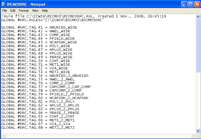
=========OPEN_THE_TAG_FILE=======c:\icwin\BICMOS\BICMOSDRC.TAG============ !Rule file
C:\ICWIN\BICMOS\BICMOSDRC.RUL, created 1 Nov., 2008, 00:45:19 GLOBAL
#DRC.RULES="C:\ICWIN\BICMOS\BICMOSDRC"
GLOBAL #DRC.TAG.41 = NBURIED_WIDE GLOBAL #DRC.TAG.42 = NWEL_WIDE GLOBAL #DRC.TAG.43 = COMP_WIDE GLOBAL #DRC.TAG.44 = PFIELD_WIDE GLOBAL #DRC.TAG.45 = NCAPSNK_WIDE GLOBAL #DRC.TAG.46 = POLY_WIDE GLOBAL #DRC.TAG.47 = NPLUS_WIDE GLOBAL #DRC.TAG.48 = PPLUS_WIDE GLOBAL #DRC.TAG.49 = PBASE_WIDE GLOBAL #DRC.TAG.50 = CONT_WIDE GLOBAL #DRC.TAG.51 = MET1_WIDE GLOBAL #DRC.TAG.52 = VIA_WIDE GLOBAL #DRC.TAG.53 = MET2_WIDE GLOBAL #DRC.TAG.54 =
NBURIED_2_NBURIED GLOBAL #DRC.TAG.55 = NWEL_2_NWEL GLOBAL #DRC.TAG.56 = COMP_2_COMP GLOBAL #DRC.TAG.57 =
CAPCOMP_2_CAP_COMP GLOBAL #DRC.TAG.58 =
CAPCOMP_2_COMP GLOBAL #DRC.TAG.59 =
PFIELD_2_PFIELD GLOBAL #DRC.TAG.60 =
NCAPSNK_2_NCAPSNK GLOBAL #DRC.TAG.61 = POLY_2_POLY GLOBAL #DRC.TAG.62 = NPLUS_2_NPLUS GLOBAL #DRC.TAG.63 = PPLUS_2_PPLUS GLOBAL #DRC.TAG.64 = PBASE_2_PBASE GLOBAL #DRC.TAG.65 = CONT_2_CONT GLOBAL #DRC.TAG.66 = MET1_2_MET1 GLOBAL #DRC.TAG.67 = VIA_2_VIA GLOBAL #DRC.TAG.68 = MET2_2_MET2 GLOBAL #DRC.TAG.69 =
NWEL_2_NPLUS_COMP GLOBAL #DRC.TAG.70 =
NWEL_2_PPLUS_COMP GLOBAL #DRC.TAG.71 =
NCAPSNK_2_COMP GLOBAL #DRC.TAG.72 =
NCAP_COMP_2_NWEL GLOBAL #DRC.TAG.73 = POLY_2_COMP GLOBAL #DRC.TAG.74 = NPLUS_2_NWEL GLOBAL #DRC.TAG.75 =
PPLUS_2_NCAPSNK GLOBAL #DRC.TAG.76 =
PPLUS_2_NPLUS_COMP GLOBAL #DRC.TAG.77 =
NBURIED_IN_NWEL GLOBAL #DRC.TAG.78 =
PPLUS_COMPIN_NWEL GLOBAL #DRC.TAG.79 =
GATE_COMP_IN_NWEL GLOBAL #DRC.TAG.80 =
PBASE_COMP_IN_NWEL GLOBAL #DRC.TAG.81 =
NWEL_IN_PFIELD GLOBAL #DRC.TAG.82 =
NCAPSNK_IN_NPLUS GLOBAL #DRC.TAG.83 = COMP_IN_NPLUS GLOBAL #DRC.TAG.84 = COMP_IN_PPLUS GLOBAL #DRC.TAG.85 =
NPLUS_COMP_IN_BASE GLOBAL #DRC.TAG.86 =
PBASE_COMP_IN_BASE GLOBAL #DRC.TAG.87 = CONT_IN_POLY GLOBAL #DRC.TAG.88 =
CONT_IN_NPLUS_COMP GLOBAL #DRC.TAG.89 =
CONT_IN_PPLUS_COMP GLOBAL #DRC.TAG.90 = CONT_IN_MET1 GLOBAL #DRC.TAG.91 = VIA_IN_MET1 GLOBAL #DRC.TAG.92 = VIA_IN_MET2 GLOBAL #DRC.TAG.93 =
ACUTE_ANGLE_WARNINGS GLOBAL #DRC.ERROR.WIRES = "20" !There were no error polygon
output layers in this rule file. REMOVE #DRC.ERROR.POLYGONS GLOBAL #DRC.ERROR.LAYERS = "20+99" GLOBAL #DRC.OUTPUT.LAYERS = "20" GLOBAL #DRC.LAYERS = "20+99" GLOBAL #DRC.MAX.TAG=93
=========NEED_A_NEW_LVS_FILE=======c:\icwin\BICMOS\CONTROL_BiCMOS.LVS============ *************************************************************************** **
FILE TYPE : CONTROL FILE FOR
LVS
** **
FILE NAME :
control.lvs
** *************************************************************************** *************************************************************************** **
DIRECTORY PATH & FILE NAME
EXTENSION
** *************************************************************************** OUTPUT_DIRECTORY_PATH = "results" OUTPUT_FILE_NAME_EXTENSION_FOR_LVS
= "lvs"
*************************************************************************** **
COMPARISON TYPE & FILE
FORMAT
** *************************************************************************** TYPE_OF_COMPARISON = LVS SCHEMATIC_FILE_FORMAT = SPICE TOP_LEVEL_SUBCKT_IN_SCHEMATIC_FILE
= TOPCELL
SECOND_SCHEMATIC_FILE_FORMAT =
pspice TOP_LEVEL_SUBCKT_IN_SECOND_SCHEMATIC_FILE
= ss
**********************************
MOSFETs ******************************** SCALE_MOSFET_LENGTH_AND_WIDTH =
1E6 MERGE_SERIES_MOSFETS = YES MERGE_PARALLEL_MOSFETS = YES MERGE_DISSIMILAR_SIZED_MOSFETS =
YES MERGE_MOSFET_CHAINS = YES MERGE_OUT_OF_ORDER_MOSFET_CHAINS
= NO COLLAPSE_SERIES_LOGIC_MOSFETS = NO COLLAPSE_PARALLEL_LOGIC_MOSFETS =
NO COLLAPSE_DISSIMILAR_SIZED_MOSFETS
= NO MATCH_MOSFET_MODELS = NO MATCH_MOSFET_PARAMETERS = YES IGNORE_UNCONNECTED_MOSFETS = NO IGNORE_ONE_TERMINAL_CONNECTED_MOSFETS
= NO IGNORE_TWO_TERMINALS_CONNECTED_MOSFETS
= NO IGNORE_SHORTED_MOSFETS = NO IGNORE_MOSFET_IF_GATE_PIN_IS_TIED_TO_CRITICAL_NET
= NO IGNORE_MOSFET_IF_SOURCE_AND_DRAIN_PINS_ARE_TIED_TO_CRITICAL_NET
= NO
**********************************
BIPOLARs ******************************* NUMBER_OF_PINS_FOR_BIPOLAR = 3 SWAP_EMITTER_AND_COLLECTOR_TERMINALS
= NO MERGE_SERIES_BIPOLARS = NO MERGE_PARALLEL_BIPOLARS = YES MERGE_BIPOLAR_CHAINS = NO MERGE_OUT_OF_ORDER_BIPOLAR_CHAINS
= NO COLLAPSE_SERIES_LOGIC_BIPOLARS =
NO COLLAPSE_PARALLEL_LOGIC_BIPOLARS
= NO COLLAPSE_DISSIMILAR_SIZED_BIPOLARS
= NO MATCH_BIPOLAR_MODELS = NO MATCH_BIPOLAR_PARAMETERS = YES IGNORE_UNCONNECTED_BIPOLARS = NO IGNORE_ONE_TERMINAL_CONNECTED_BIPOLARS
= NO IGNORE_TWO_TERMINALS_CONNECTED_BIPOLARS
= NO IGNORE_SHORTED_BIPOLARS = NO IGNORE_BIPOLAR_IF_BASE_PIN_IS_TIED_TO_CRITICAL_NET
= NO
########################################################################### ##
CONTROL FILE :
CONTROL_BiCMOS.LVS
## ##
FIRST NETLIST :
ALL_GEOS_LVS_SCH.NET
## ##
SECOND NETLIST :
ALL_GEOS_LVS_LAY.NET
## ##
DATE & TIME :
Thu Nov 06 01:10:30
2008 ## ##
ELAPSED TIME : 0
sec
## ##
MEMORY ALLOCATED :
24000
bytes
## ##
LVS VERSION :
1.15
## ########################################################################### ########################################################################### ##
<<@>> Indicates SERIES device
merge.
## ##
<<&>> Indicates PARALLEL
device
merge.
## ##
<<M>> Indicates Merge
device.
## ##
<<P>> Indicates Pseudo
device.
## ##
<<V>> Indicates Virtual
net.
## ##
<<?>> Indicates Device
Parameter value set by user. ## ##
<<number>> Indicates Total Number of Devices
included. ## ########################################################################### ########################################################################### ##
Number of matched
devices =
9
## ##
Number of matched
nets
=
8
## ########################################################################### ########################################################################### ##
The following DEVICES were
matched.
## ##
**POTENTIAL MATCHES
FOUND**
## ###########################################################################
SCHEMATIC
|
LAYOUT
|
|
#
:1
| #
:1
MN1
|
274
X
:0
Y
:0
| X
:10
Y :79
MODEL
:NMOS TYPE
:NMOS | MODEL
:NMOS TYPE
:NMOS LENGTH
:1 WIDTH
:1 | LENGTH
:1 WIDTH
:1
|
#
:2
| #
:2
MP1
|
821
X
:0
Y
:0
| X
:-42
Y :74
MODEL
:PMOS TYPE
:PMOS | MODEL
:PMOS TYPE
:PMOS LENGTH
:1 WIDTH
:1 | LENGTH
:1 WIDTH
:1
|
---------------------------**
PARAMETER ERROR **--------------------------- #
:3
| #
:3
QN1
|
280
X
:0
Y
:0
| X
:-53
Y :16
MODEL
:V_NPN TYPE
:NPN | MODEL
:V_NPN TYPE
:NPN AREA
:1
| AREA
:9.1
|
---------------------------**
PARAMETER ERROR **--------------------------- #
:4
| #
:4
QN2
|
836[M,10]
X
:0
Y
:0
| X
:-53
Y :-26 MODEL
:V_NPN TYPE
:NPN | MODEL
:V_NPN TYPE
:NPN AREA
:10
| AREA
:91
|
---------------------------**
PARAMETER ERROR **--------------------------- #
:5
| #
:5
QP1
|
59
X
:0
Y
:0
| X
:-27
Y :40
MODEL
:L_PNP TYPE
:PNP | MODEL
:L_PNP TYPE
:PNP AREA
:1
| AREA
:6.76
|
---------------------------**
PARAMETER ERROR **--------------------------- #
:6
| #
:6
QP2
|
60
X
:0
Y
:0
| X
:-9
Y :40
MODEL
:L_PNP TYPE
:PNP | MODEL
:L_PNP TYPE
:PNP AREA
:1
| AREA
:6.76
|
#
:7
| #
:7
C1
|
279
X
:0
Y
:0
| X
:68
Y :76
MODEL :CAPACITOR TYPE
:CAP | MODEL
:CAPN TYPE
:CAP VALUE
:1e-012 P:0
A:0 | VALUE :1.8655e-011
P:55 A:186
|
---------------------------**
PARAMETER ERROR **--------------------------- #
:8
| #
:8
RB1
|
275
X
:0
Y
:0
| X
:6
Y :-7
MODEL :RESISTOR
TYPE :RES | MODEL
:RESB TYPE
:RES VALUE
:61000
L:0
W:0 | VALUE
:61210 L:91.8
W:1.5
|
---------------------------**
PARAMETER ERROR **--------------------------- #
:9
| #
:9
RB2
|
837[M,3]
X
:0
Y
:0
| X
:19
Y :-7
MODEL :RESISTOR
TYPE :RES | MODEL
:RESB TYPE
:RES VALUE
:180000 L:0
W:0 | VALUE
:183630 L:275.4
W:1.5
|
########################################################################### ##
The following NETS were
MATCHED.
## ##
**POTENTIAL MATCHES
FOUND**
## ###########################################################################