THE LMC2001 STORY
In the days of vacuum tubes, a method was found to use
relays
to
chop a DC signal into an AC signal, which then could gained up and
rechopped back into a DC signal. Since then, vacuum tubes have been
replaced by transistors and relays have be replaced by CMOS switches
which can come close to behaving like ideal switches.
CMOS SWITCHES
___ ___
___|IN2|/|___| _|_ CMOS AMP
| |___|\| : /1/F\
___
| ___ : \___/ |\
|IN1|_____/|\_|IN1|
: |___|+\ ____
|___| | |
|___| :
| \___|OUT1|
| |
: | /
|____|
| | ___
: __|-/
|__/|\_|IN1|/|___ | |/
| |___|\| |_____|
___
| ___
|IN2|_____|__|IN2|
|___| |___|
"Chopper Amplifiers" use in effect ideal switches to
modulate
desired
signal away from undesired signal. The switching of the desired input
signal between the inputs is just multiplexing or modulating the desired
input to the frequency of the chopping clock. CMOS switches don't have
offset and have only flat band noise
defined by their ON resistance.
The Chopping of the input can place the desired signal well above
the 1/f corner of any amplifier which follows it.
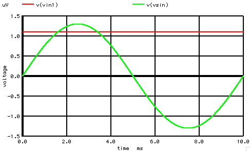
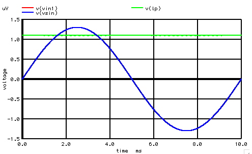
To see how this is done,
suppose the desirable signal is DC
and
the undesired signal is AC like 1/f noise.
CMOS SWITCHES
___ ___
___|IN2|/|___| _|_ CMOS AMP
| |___|\| : /1/F\
___
| ___ : \___/ |\
|IN1|_____/|\_|IN1|
: |___|+\ ____
|___| | |
|___| :
| \___|VSUM|
| |
: | /
|____|
| | ___
: __|-/
|__/|\_|IN1|/|___ | |/
| |___|\| |_____|
___
| ___
|IN2|_____|__|IN2|
|___| |___|
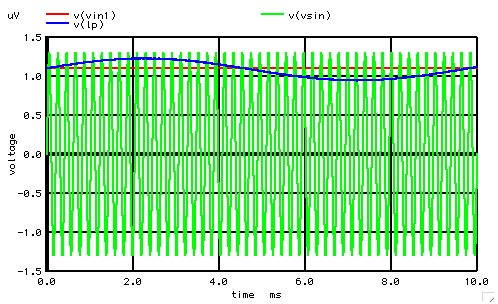
CMOS switches have no offset. So if the desired signal gets
chopped
before being added to the undesirable AC signal, the following is
the result.
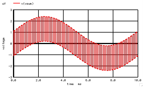
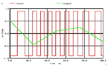
So what happens when this combined signal gets chopped or
multiplexed
by the same clock again?
______
______
______
VIN1
| |OUT1 | _
|VSUM |
| ____
_____|\| \ / |____|\|
/ |_______|\| \ / |___|OUT2|
_|_ |/| X
| |/| _\
| |/| X
| |____|
/VIN\ | / \
|
|______| | / \ |
\___/
|______| ^
BSUM |______|
_|_
^ BMUX1
/_\
^ BMUX2
///
/_\
_|__ VSIN /_\
|_____ /_
\ |
_|_ | // \
\ |
VCLK /_ \
| \
\_// |
/|
| \ |
\____/
|
\ |_|/ |
_|_
|
\___/ |
///
|
| |________________________|
_|_
///
What actually happens is that the desired signal comes out
unchanged and now the undesirable signal is being modulated
or multiplexed around the chopper clock frequency.
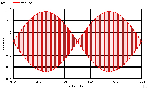
This makes it convenient to just add a lowpass filter to
remove
the undesirable signal from the desirable.
______
______
______ OUT2
VIN1
| |OUT1 | _
|VSUM |
|
___
_____|\| \ /
|____|\| / |_______|\| \ / |___/\
/\ /\_______|LP |
_|_ |/| X
| |/| _\
| |/| X
| \/ \/ _|_ |___|
/VIN\ | / \
|
|______| | / \
| ROUT ___
\___/
|______| ^
BSUM
|______|
_|_ COUT
_|_ ^
BMUX1
/_\
^ BMUX2 ///
///
/_\
_|__ VSIN
/_\
|_____ /_
\ |
_|_ | // \
\ |
VCLK /_
\ | \
\_// |
/| | \ |
\____/
|
\ |_|/ |
_|_
|
\___/ |
///
|
| |________________________|
_|_
///
Of course it is desirable that the chopper clock should be
set
high enough above the bandwidth of the desired signal to allow
for alias and filtering requirements.
There is a catch. If
anything gets into the signal path that
comes
close enough to the chopper clock, it can get aliased.
In the case above the sine wave is getting close enough to the
chopper frequency to get aliased down to a lower frequency.
A common way the industry avoids this problem is to spread spectrum
the clock frequency by a random signal.
If the clock can be randomly frequency modulated, this will
spread
the spectrum out.
If the same randomize clock is fed to both switching
blocks, the
desired input will come through unchanged. But an undesirable
signal will now have to have the exact same randomness as the
chopper clock in order to create interference. This how cell phones
work.
The goal of the LMC2001 design was build a "perfect Op Amp".
A perfect Op Amp has no input bias current and no input
offset and no input noise. Designing a CMOS Op Amp with a
hugh input stage tends to go in this direction. Both noise
and offset decrease by the square root of transistor area.
And CMOS input Op Amps have the input bias current of glass.
So the lowering of input noise voltage does not mean an increase
in input noise current. Still there is that problem with
1/f noise. An even if laser trim gets added, input offset
will still tend to drift with time and temp.
___________
| + _|_ +/- .1uV
=> +/-10mV = 100dB
| 1mV /VOS\
| -\___/ |\
B100dB
_|__ VIN
|______|+\
___
/_ \ 10KHz
INP | \___________|OUT|
// \
\ INN |
/ | |___|
\ \_//
CDCB
__|-/ |
\____/ ___|
|/ |
_|_ 10pF _|_
|
|
/// ___
|__/\ /\ /\__|
_|_ \/ \/
/// RDCB needs 1.6E12
Suppose one wants to do the chopping at 10KHz and want to
have
an easy time looking a signals well below a micro volt. This
implies that a large AC gain needs to be taken on board the chip.
For instance, the input CMOS switches will convert a 100nV DC input
into an +/- 100nV AC signal. This signal needs to enough gain
such that it is well above the typical transistor differential input
offset level. Taking large AC gain has done in FM radios since the
days of vacuum tubes
A typical amplifier will have a typical input offset
of a
few millivolts. The FM radio solution
is to provide an RC
feedback to the negative input of a gain stage. At DC, the
loop gain will be one. If the RC time constant is high enough,
enough gain will be taken of the desired input signal
frequency.
___________
| + _|_ +/- .1uV
=> +/-10mV = 100dB
| 1mV /VOS\
| -\___/ |\
B100dB
_|__ VIN
|______|+\
___
/_ \ 10KHz
INP | \___________|OUT|
// \
\ INN |
/ | |___|
\ \_//
CDCB
__|-/ |
\____/ ___|
|/ |
_|_ 10pF _|_
|
|
/// ___
|__/\ /\ /\__|
_|_ \/ \/
/// RDCB needs 1.6E12
It would also be desirable that the 100dB gain should be
taken
without the need of external components. An on chip capacitor
around 10pF is a good
size. Now to have a gain of 100dB at 10Khz,
the resistor value is going to
need to be large.
But there is even a better way to do this.
Suppose instead an
integrator is used to handle the input offset of the 100dB gain
stage.
___________
| + _|_ +/- .1uV
=> +/-10mV = 100dB
| 1mV /VOS\
| -\___/ |\
B100dB
_|__ VIN
|______|+\
___
/_ \
10KHz INP | \___________|OUT|__________
// \
\ INN |
/ CINT
|___| |
\ \_//
___________|-/
__||____
|
\____/
| |/
OUT2 | ||
| |
_|_
|
/| ^
| /| | RINT |
///
| / |_ /_\
| /-|_|_/\ /\ /\_|
|__/ | |________|___|__/ |INN2 \/ \/
\
|
\ |
BINV\ |__
BINT \+|__
\|
_|_
\| _|_
///
///
An integrator has the ability to have large DC
gain. This
will reduce the amount of input offset that appears at the output.
In this "system simulation", the integrator has infinite
gain at
DC.
At 10kHz the gain needs to be open loop at 100dB. This means the
100dB gain stage needs to have unity gain at around 10mHz.
All that is needed now is to be able to build an on chip
integrator
which has it unity gain frequency around 10mHz.
Since the negative feedback is much greater than one, a 1mV
input
offset will get attenuated at the output by the DC gain.
The ability to build a subHertz integrator is a fringe
benefit
of the BiCMOS process. In order the have CMOS work, the lifetime of
minority carriers needed to be increase by a factor of around
a thousand over and above what was standard in the old analog
bipolar process. This means that bipolar transistor can now
work at a thousand times lower current than before. And BiCmos
also makes it possible to have buffers with the input impedance
of glass.
VCC ^
VCC ^
R1 /_\
/_\ __/\ /\ /\__|
| | \/ \/
__|_____/|\_______
|
| |
R2 ->QP1 | QP2
<- R3
__________/\ /\ /\___`|_____|____|'____/\ /\ /\_
|
\/ \/ _'| VPB
|`_ \/ \/ |
|
VNC1
|
|
|
|
_________________/|\_______________|
_______|
|
|
| ^ ^
| |
|
|
| /_\ /_\
| |
| |
_____________| |
| | |
| | |
VNC2 |
<- ->
| |
| |
|
| || ||
| |
| |
|
|_||MP1 MP2||_| |
| |
|
| ||_ _||
| |
| |
|
| | |
| |
|_/|\__/|\_______ ->
| |
<- |
| |
| || |VG3 |
|| |
| |
| MP3||_|
|_||MP4 |
| |
| _|| | VG4|
||_ |
_| |_
| | _|_ _|_
| |
__|'QN1
QN2`|_ | VG5| / _ \ / _ \
|VG6 |
|
|`-> <-'| | |
| \/ \/ \/ \/ | |
VIN |
|____| _|_ -> | /\_/\
/\_/\ | <-
_|_ |
/// || | \___/ \___/ | ||
/_ \
VNE_|_ MP5 ||_|
_|_ _|_ |_||MP6
// \ \ / _
\ _|| |
/// /// | ||_
\ \// \/
\/I1 | |
I2 I3
| |
\___/
/\_/\ 1nA
| |_______||_______| |
_|_
\___/ |
_|_ ||
_|_ |
///
_|_ | / _
\ C0 / _ \ |
/// | \/
\/ 10pF
\/ \/ |
|
/\_/\
/\_/\ |
|
\___/
\___/ |
| _|_ I4 I5
_|_ |
|
///
/// | OUT2
OUT1
|
| _________
|_/\ /\ /\___/\ /\
/\__|_| |
___
| \/ \/ _|_ \/
\/ |OUT1-OUT2|__|OUT|
| R4
/// R5
| | |___|
|____________________________|
|
|_________|
The SubHertz integrator
can be build using standard
geometries
found in a BiCmos process. The simulations is showing a pole for
the integrator around 3mHz. This number needs to be taken with a
grain of salt because all BiCMOS processes need to get modeled
correctly.
This SubHertz integrator found three powerful applications
inside
the LMC2001. First the chopper input
signal could be gained up
enough such that a standard four quadrant multiplier could be used
to perform the second modulation.
VCC ^
VCC ^
R1 /_\
/_\ __/\ /\ /\__|
| | \/ \/
__|_____/|\_______
|
| |
R2 ->QP1 | QP2
<- R3
__________/\ /\ /\___`|_____|____|'____/\ /\ /\_
|
\/ \/ _'| VPB
|`_ \/ \/ |
|
VNC1
|
|
|
|
_________________/|\_______________|
_______|
|
|
| ^ ^
| |
|
|
| /_\ /_\
| |
|
| _____________|
| | |
|
|
| | VNC2
| <- ->
| |
|
|
|
| || ||
| |
|
|
|
|_||MP1 MP2||_| |
|
|
|
| ||_ _||
| |
|
|
|
| | |
| |
|_/|\__/|\_______ ->
| |
<- |
| |
| || |VG3 |
|| |
| |
| MP3||_|
|_||MP4 |
| |
| _|| | VG4|
||_ |
_| |_
| | _|_ _|_
| |
__|'QN1
QN2`|_ | VG5| / _ \ / _ \
|VG6 |
| |`->
<-'| | | | \/ \/ \/
\/ | |
|
|____| _|_ -> | /\_/\
/\_/\ | <-
| |
/// || | \___/ \___/ | ||
|
VNE_|_ MP5 ||_|
_|_ _|_ |_||MP6
| /
_ \ _|| |
/// /// | ||_
| \/
\/I1 | |
I2 I3
| |
|
/\_/\ |
|_______||_______| |
|
\___/ |
_|_ ||
_|_ |
|
_|_ | / _
\ C0 / _ \ |
|
/// | \/
\/ \/
\/ |
|________________
|
/\_/\
/\_/\ |
| |
\___/
\___/ |
| | _|_ I4
I5 _|_ |
____
| |
///
/// | OUT2
|
_|_ |
|
| ____
| /VOS\INP |\
| |_/\ /\ /\___/\ /\
/\__|_| | ___
| \___/ __|+\
| | \/ \/ _|_ \/
\/ | |_|INN|
| |____| |
\__| | R4
/// R5
|BDIF| |___|
VIN
| |
/ | |____________________________|
| |
_|_ INN __|-/
|
|____| |
/_ \ |
|/ |
____
|
// \ \
|
|__|OUT0|
|
\ \// |
B100dB
|____|
|
\___/
|_________________________________________________|
_|_
///
A fringe benefit to the gain of the 100dB gain block is the
desired signal at 10KHz can have full 100dB gain while the
1/f noise of the 100dB gain stage will have considerably less.
A second fringe benefit to the SubHertz integrator is that now
the output of the chopper can be integrated as opposed to just
lowpass filtering. This
makes it possible to build a composite
amplifier.
A third benefit is that it is now possible to take enough gain on
chip to actually use shot noise to frequency modulate the chopper
clock. Now the option exists to spread spectrum using real
analog randomness as oppose
to using digital pseudo randomness.
^
^ VCC VP R2
/_\VCC
/_\ ____/\ /\ /\__|
| | \/ \/
|____/|\____
QP2 | | |QP3
VP1E
-> |
<- R3 VP4E
_/\ /\
/\____`|_|_|'___/\ /\ /\_
| \/
\/ _'| |`_
\/ \/
|
^ VCC
|
R1
|
|
| VC
R4 /_\
-> VP1B |
C1 | VP4B
<-
_/\ /\ /\__|
QP1 `|_________|____||___|________|'
QP4 |
\/ \/
_'|
| | || |
|
|`_ |
_|_ I1
| | |
|I2
_|_ _|_
///
_|_ | |
_|_
/// /VC \
/ _ \ | | / _
\
\___/
\/ \/ | | \/
\/
_|_
/\_/\ | |
/\_/\
///
\___/ | | \___/
_|_ | | _|_
/// | |
/// |\ BDIF
|____/|\_____________|+\ INN BOUT
| |___________ |
\______|\ _ _ INP
_|
|_ |
| / - | \/ \/ \_
__|'QN1 QN2`|__
|__|-/ ___| /\_/\_/ |
_| |`-> <-'|
| |/
|+ |/ |
/// |_____|
|_______________|____________|
_|_
VNE
|
/ _
\
|_/\ /\ /\_
\/ \/
I3
\/ \/ _|_
/\_/\
R5 ///
\___/
_|_
///
The ability to do a analog spread spectrum had some further
benefits.
There was the option to run
the clock without using CMOS logic. The BiCMOS
process allows very small transistors to run at very high speeds at
very low supply currents. The whole clock logic can be run fully
differentially at a constant DC current.
The waveforms to the oscillator above are standard.
The supply current varies slightly due to early voltage.
The supply current glitches
of a minimum geometry inverter is shown
along side for reference. There is no need to have digital supply
glitches because the differential logic can be run at very low DC
current levels. Slower rise and fall times also tend to reduce
clock feedthru in CMOS switches.
This constant DC current oscillator can also be frequency
modulated.
At one time, the oscillator in the LMC2001 was subject to spread
spectrum using analog shot noise.
CIN
VIN
__||___
^
| || |
/_\ |\ BCHOP
RINT | |
|__|
\
| |\ |
|
\____/\ /\ /\_|_|-\ | ___
|
/ \/ \/
| \__|___|OUT|
__| /
VCHOP INN |
/ |___|
_|_
|/
__|+/BINT
\
/
_|_ |/
V
VIN2
///
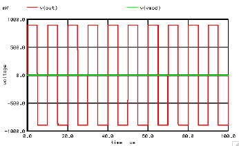
Integrating the chopper output
signal makes the chopper stage
look like a low frequency Op Amp. In this case the undesirable
signal is being chopped up to 10KHz and the integration is set
to have unity gain at 1kHz.
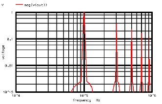
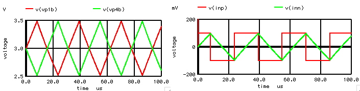
The chopper stage multiplexes the desired input signal,
gains it up by 100dB, then multiplexes it again to
convert it back to its original form. So the idea is to just
take gain to the desired input signal. If this signal
is fed into a gm stage and then on to an integrator stage,
it can be thought of a just being a low frequency Op Amp.
The unity gain cross needs to be set at least an order
of magnitude below the chopper frequency. The undesirable
signal of the 100dB gain stage is now be multiplexed to the
chopper frequency and will appear somewhat like what is
shown above.
________________________________
|
|
|
BOTA
|\ |
|
____|+\ |
|___|\ _ _ _|_ |
\_______|
VIN - | \/ \/
\_ /// | /
| ___
________| /\_/\_/
|_______|-/ |__|OUT|
_|__ +
|/ INN2| |/
BOPA | |___|
/_
\
| |
// \
\
|__||________|
\
\_//
| || CCOMP |
\____/
| |
_|_
|_/\ /\ /\_|
///
RAV\/ \/
Well, an Op Amp with a 1KHz unity gain band width might
have a limited amount of application. What if a companion
Op Amp could be hooked up along side it which had a limited
amount of open loop gain.
When designing an Op Amp, limited
open loop gain usually
comes without trying. Gain is often limited by things
like early voltage.
_________________________________________
|
|
|
BOTA
|\ |
|
____|+\ |
|____________|\
_ _ _|_ | \_______|
VIN |
- | \/ \/ \_ /// |
/ | ___
___________/|\___| /\_/\_/
|_______|-/ |__|OUT|
_|__ | | +
|/ INN2| |/
BOPA | |___|
/_ \ |
|
| |
// \ \ |
|
|__||________|
\ \_// |
|
RPZC | || CCOMP |
\____/ |
|
| |
_|_ |
| _/\ /\
/\_|_/\ /\ /\_|
/// |
| | \/
\/ RAV\/ \/
| |
|_________________
|
___|
|
|
|
CINT __||___|
|
|
| || |
|
| |\ BCHOP RINT
| |OUT2
|
|__|+\
| |\ |
| | \____/\ /\
/\_|_|-\ |
| | /
\/ \/ | \__|
|_____|-/
INN | /
|/
__|+/
_|_ |/
///
When the "Chopper Op Amp" is hooked up along side, it can
provide additional gain at the lower
frequencies.
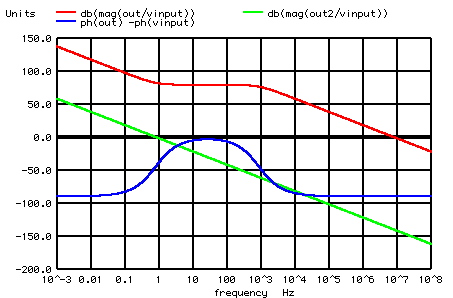
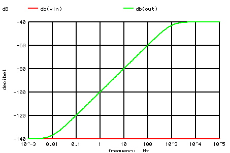
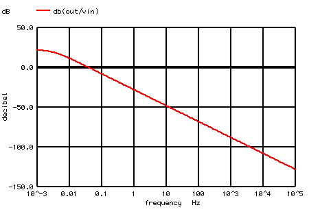
The gain/phase plot above shows what happens when the value
of the integration capacitor CINT is chosen to dominate the
overall gain below 1Hz.
When the integration capacitor CINT is chosen to dominate gain
below 1Hz, the two parallel Op Amps behave like a single
one pole Op Amp. Effectively you have a pole zero cancellation.
The best place to see this cancellation is by observing how well
the phase remains at 90 degrees.
But the "Chopper Op Amp" is doing
a little more that just
adding some
additional open loop gain. Consider where undesirable signals like
input offset and 1/f noise resides in the high frequency Op Amp path
(nhfp) and the low frequency Op Amp path (nlfp). The high frequency
path (nhfp) has normal offset and 1/f noise. The low frequency path
(nlfp) doesnot offset and 1/f noise. But it does have all its
undesirable signal being modulated around the chopper frequency of
10KHz.
_________________________________________
|
|
|
BOTA
|\ |
|
____|+\ |
|____________|\
_ _ _|_ | \_______|
VIN |
- | \/ \/ \_ /// |
/ | ___
___________/|\___| /\_/\_/
|_______|-/ |__|OUT|
_|__ | | +
|/ INN2| |/
BOPA | |___|
/_ \ |
|
| |
// \ \ |
|
|__||________|
\ \_// |
|
RPZC | || CCOMP |
\____/ |
|
| |
_|_ |
| _/\ /\
/\_|_/\ /\ /\_|
/// |
| | \/
\/ RAV\/ \/
| |
|_________________
|
___|
|
|
|
CINT __||___|
|
|
| || |
|
| |\ BCHOP RINT
| |OUT2
|
|__|+\
| |\ |
| | \____/\ /\
/\_|_|-\ |
| | /
\/ \/ | \__|
|_____|-/
INN | /
|/
__|+/
_|_ |/
///
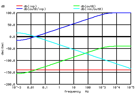
Now look at the gain to each path. Below 1kHz, the low
frequency
path (glfp)
has higher gain than the high frequency path (ghfp).
That means it is dividing any error signal in the high frequency
Op Amp by the amount of gain that it is contributing. If it has
a very large amount of gain at DC, then the input offset will be
greatly reduced. The same applies to 1/f noise.
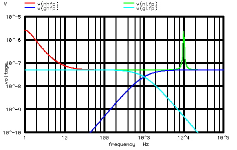
Above 1kHz, the low
frequency Op Amp's own integrator
is attentuating all the chopper frequency's undesirable
signal. It is set to only be able to dominate the signal
path below 1kHz.
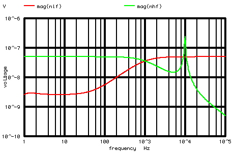
Below 1kHz, chopper Op Amp will dominate offset and noise.
Above 1kHz, the chopper Op Amp is no longer dominate and
noise will be dominated by the high frequency Op Amp. Raising
the clock frequency will attenuate the chopper's
undesirable signal further. The LMC2001's clock frequency
was intended to later be increased above 10KHz.
Flat band noise is defined by thinking of gm in V/I terms
of input impedance. The two Op Amps where designed to
have around the same flat band noise. The LMC2001 was
at one time design to operate exactly like is shown above
in order to test how well the
concepts worked. Remember,
the spread spectrum circuitry was installed and there was
some inherent attenuation of 1/f noise in the 100dB
gain stage. When building something like a LMC2001, nothing
should be assumed to be working correctly. Silicon always
needs to be fully tested.
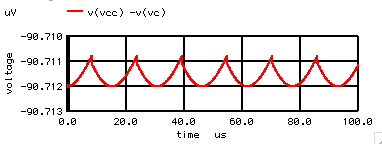
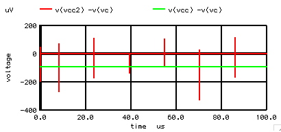
In some of the first silicon parts, the spread spectrum was cut
out to view the resulting chopper noise. With the spread spectrum
in, it did appear spread out the spike as expected. It looked
like it would be possible to bury all the chopper noise in
the high frequency Op Amp's flat band noise.
The goal was to be able to hide all chopper noise. The supply
current was measured to have low chopper noise. The spread
spectrum circuitry in the LMC2001 appeared to be working as
expected. Both amplifiers in the composite amplifier appeared
to be able to bury each others undesirable signal in their
flat band noise. Input referred noise voltage was working as
expected. There was now the question of input noise current.
R1
___
VCC ^
_/\ /\
/\_|IN1|_____________________
/_\
_|_ \/ \/
|___|
|
|
|
///
^ _| ^
_|
|
|_|| MN1 |_||
MN2 |
||__
||__
__| MN6
CLK1 ||->
CLK2||-> IN3 _| |_
|
|________||NM5 ||_
|
| ||______|| |
|___________/|\___ ||-> <-|| |
CLK2
|
| |
|__| |
^ _| ^
_| | IN4 | |
|_||MN3 |_||NM4
|_____/|\______|
||__ CLK1
||__ _|_
R2
||->
||-> / _ \ V1
___
|
| \/ \/
_/\ /\
/\__|IN2|_______|____________| I1 /\_/\
_|_ \/ \/
|___|
\___/
///
_|_
///
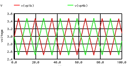
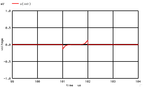
In the input switches, whenever any transistor turns on, a
matched transistor turns off. There looks like there should
be a balancing act going on. But a lot of papers and a lot
of model development has gone into reducing feedthru in a
CMOS switch.
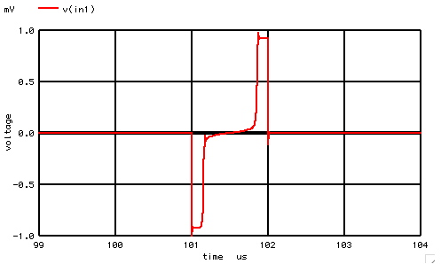
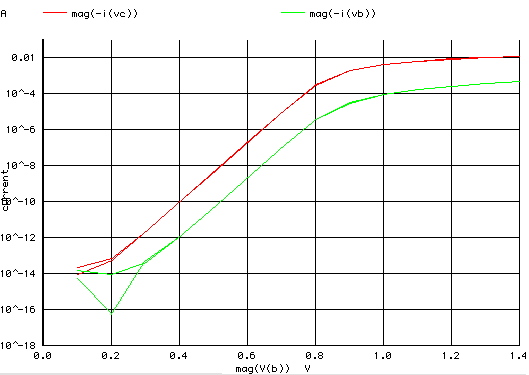
A simple simulation reveal the
following feedthru. This is one
place however where simulation results should not be trusted.
Silicon always needs to be built
to test things.
The LMC2001 provided a unique opportunity to investigate
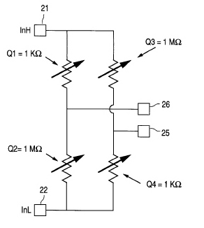
something new. The input chopper doesn't have to be a "chopper"
with switches that turn completely off. If the gate voltages where
adjusted such that the CMOS switches shifted between a 1k Ohm
ON Resistance to a 1Meg Ohm ON Resistance, the "chopper" would
still work just fine. If the full Op Amp has an effective input
offset of a few micro volts, then a 1Meg Ohm resistance across the
inputs will generate a few pico amps of DC input current.
Chopping switches go through the ultimate in non linear
operation.
They go from On to completely off. Simulates suggested that feedthru
reduction is possible. The LMC2001 was built to test this concept.
It was never tried out.
After it was confirmed that the concepts worked, management insisted
that a LMC2001 team be formed to "help"
translate working concepts into
a production worthy product. The only member on the team who has
anything resembling design experience was a PhD who was months out of
school. Somehow the Amplifier department together with the LMC2001
project got transferred to another department in another building. The
LMC2001 team eventually got full control over the project.
Check out the preTeam LMC2001
From the datasheet, it looks like the spread spectrum, the rail to rail
input, and the efforts to minimize input chopper noise current all got
eliminated.
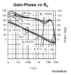
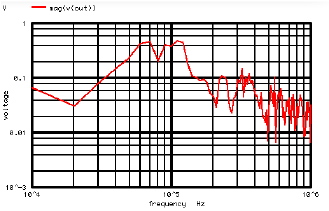
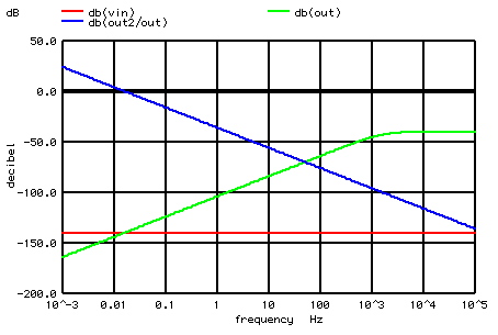
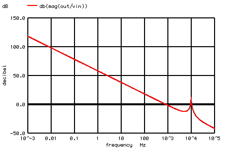
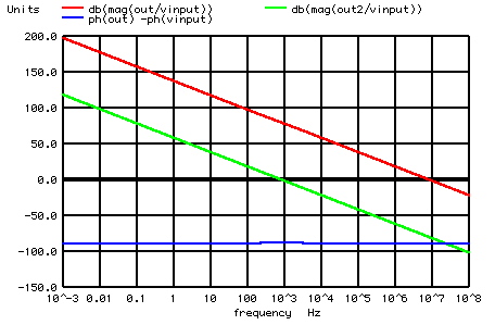
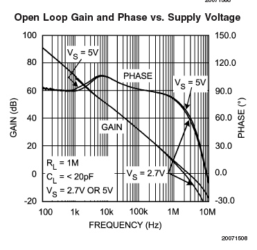
The LMC2001 gain phase plot suggest that the 1kHz transfer
between the
two amplifiers remained at 1kHz. Exactly where the low frequency open
loop
gain pole was located was at one time creating a testing problem. It
was
discovered that testing for open loop gain above 140dB was challenging
The data sheet claims a typical open loop gain of 137dB. For some reason
the data sheet is not shown it on any gain/phase graphs.
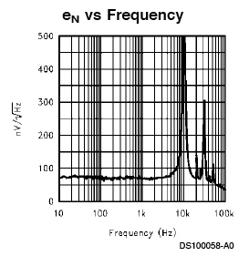
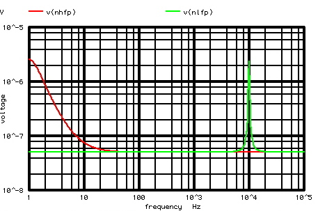
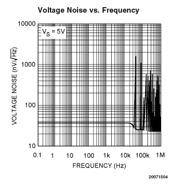
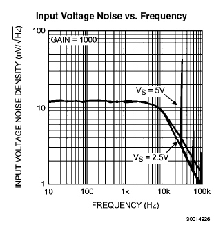
The LMC2001 noise looks much different than it used to.
Originally the
noise curve looked like it had a mild bump on it. When the spread
spectrum feature was laser cut out, the noise spike was not
an order of magnitude higher than the flatband noise. Perhaps making
the input a true chopper in addition to removing the spread spectrum
added much more chopper noise to the signal path.
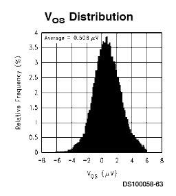
The offset distribution is the same. Having an open loop
gain higher
than 140dB means that settle time for microvolt offset can take some
expensive test time to measure. Test development had found some tricks
to address this challenge.
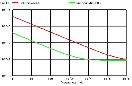
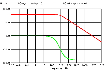
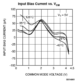
The next generation was the LMP2011 family. The noise and gain phase
of the LMP2011 suggest that the crossover frequency has been raised
to something like 10kHz. The data sheet does not give a offset
distribution. But it does shows some input bias currents.
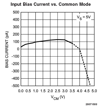
Wonder what is creating this input bias current?
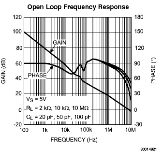
The next generation which is the LMP2021 has a gain phase curve
which shows the crossover has now been increased to maybe 50KHz.
There is still no spread spectrum added to the clock. But input
noise voltage has greatly been reduced. This noise voltage is
defined by the dynamic impedance present at the inputs. For
instance 12nV/rt_Hz represents the noise of a 9K Ohm resistor.
In a bipolar input stage, lowering input noise voltage results in
the raising input noise current. Bipolar input transistor need to
run at higher collector currents to lower their dynamic resistance.
More collector current means more base current. CMOS input stages
don't have this tradeoff. CMOS inputs allow for large input geometries
to run at large amounts of bias supply without increasing input
bias current. The input impedance and bias current should be that
of glass. The LMP2021 input bias current is a
curiosity.