TAPEOUT USING ELECTRIC
The "ELECTRIC" IC layout application does things differently. It appears that the
methods typically used for schematic entry applications has been extended to layout.
The result is that things like DRC and LVS are quite different from most other IC
layout application.
======================SCHEMATIC_ENTRY_USING_COMMON_METHOD===============
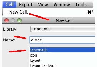
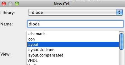
It is not uncommon that a schematic be entered as a "schematic view" of a "cell",
where the cell contains several views (icon, layout, symbol, etc).
The schematic view and the layout view are expected to completely match each
other in terms of the network hookup and component sizes.
Typical schematic entry involves selecting an object from a menu, and then
placing it into the schematic window.
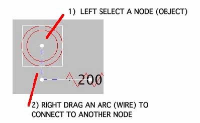
ELECTRIC is using a common hookup method where an object get left mouse selected,
and then a right mouse drag is used to form a connection from the selected object
to another object.
After two or more objects are connected, the connection is displayed.
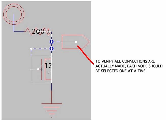
But it is very easy to think that a connection has been made when it has not.
So it is importance to verify all connections by selecting each net one at a
time to view all the connections.
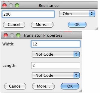
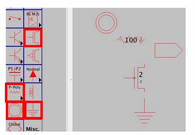
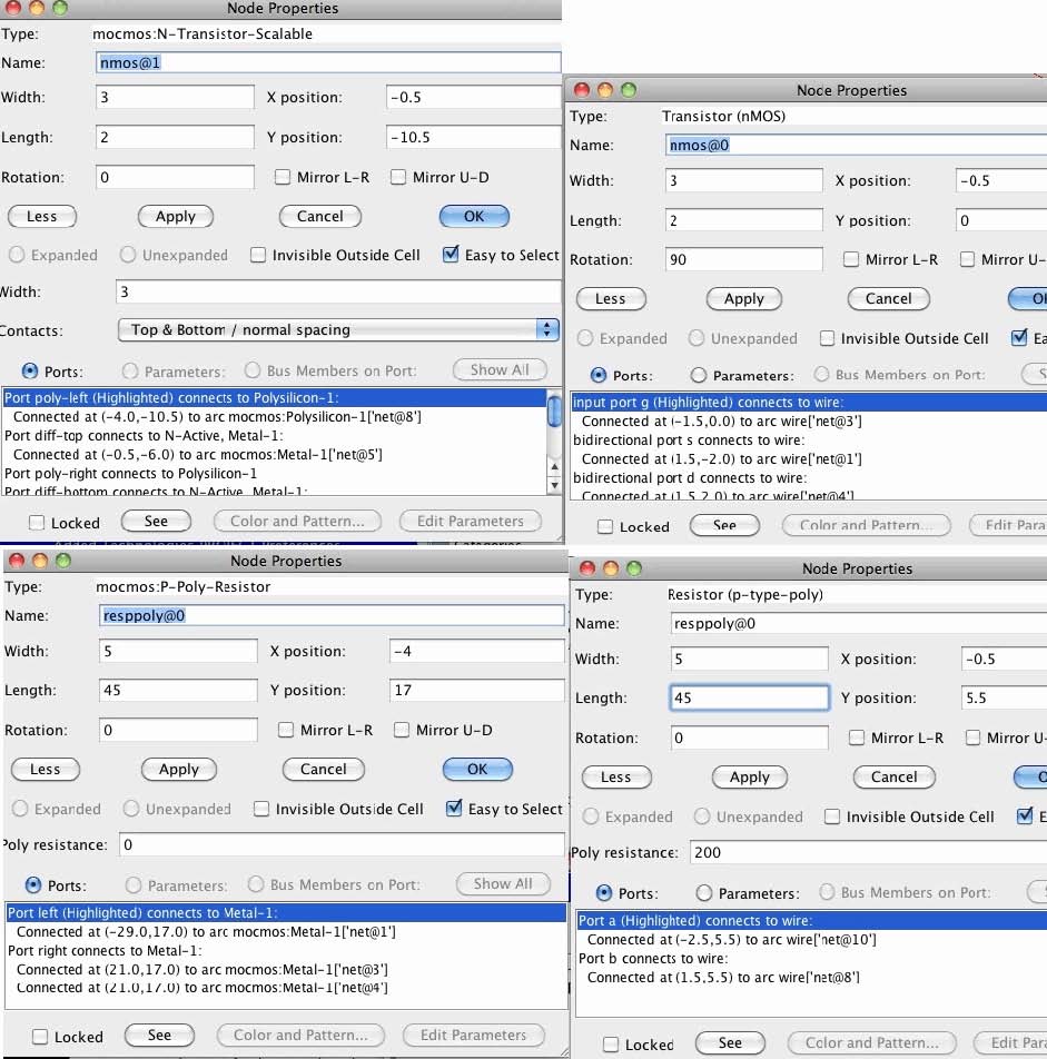
In this example the transistor and resistor are double clicked to modify some
parameters. Notice that width and length are not in
metric format.
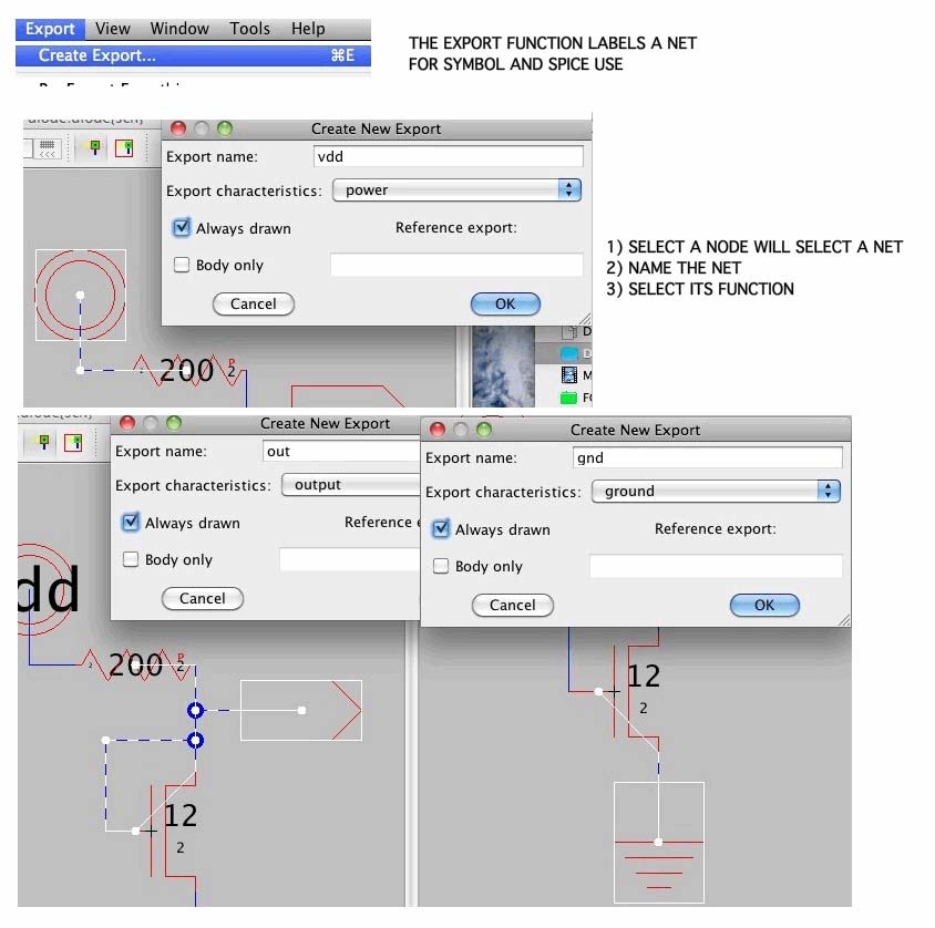
Adding labels or export ports aids in using this cell as a subcircuit,
and aids in understanding the spice netlist, and aids in matching the layout
to the schematic.
Now the schematic has the usual format with the exception that the width and
length of the transistor are in terms of layout units rather than metric units.
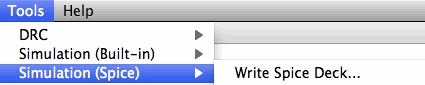
The schematic can now be exported to run on any spice platform.
The result is shown below.
*** SPICE deck for cell diode{sch} from library diode
*** Created on Thu Jun 05, 2014 12:12:03
*** Last revised on Thu Jun 05, 2014 12:28:44
*** Written on Thu Jun 05, 2014 13:14:37 by Electric VLSI Design System,
*version 9.04
*** Layout tech: mocmos, foundry MOSIS
*** UC SPICE *** , MIN_RESIST 4.0, MIN_CAPAC 0.1FF
*CMOS/BULK-NWELL (PRELIMINARY PARAMETERS)
.OPTIONS NOMOD DEFL=3UM DEFW=3UM DEFAD=70P DEFAS=70P LIMPTS=1000
+ITL5=0 RELTOL=0.01 ABSTOL=500PA VNTOL=500UV LVLTIM=2
+LVLCOD=1
.MODEL N NMOS LEVEL=1
+KP=60E-6 VTO=0.7 GAMMA=0.3 LAMBDA=0.05 PHI=0.6
+LD=0.4E-6 TOX=40E-9 CGSO=2.0E-10 CGDO=2.0E-10 CJ=.2MF/M^2
.MODEL P PMOS LEVEL=1
+KP=20E-6 VTO=0.7 GAMMA=0.4 LAMBDA=0.05 PHI=0.6
+LD=0.6E-6 TOX=40E-9 CGSO=3.0E-10 CGDO=3.0E-10 CJ=.2MF/M^2
.MODEL DIFFCAP D CJO=.2MF/M^2
.global gnd vdd
*** TOP LEVEL CELL: diode{sch}
Mnmos@0 out out gnd gnd N L=0.4U W=2.4U
Rresppoly@0 out vdd 200
.END
When the spice netlist get exported, notice that the export pins are all used.
Notice that the width and length of the NMOS transistor are now expressed in
terms of meters.
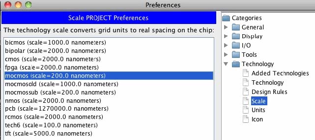
ELECTRIC actually enters the dimensions of the transistors in terms of layout
units. The scale term for this process (mocmos) is 200 nanometers per unit.
Selecting the process that is used will tell ELECTRIC which scale to use.
The schematic is saved as a "Library" file. This is a text file, and it demonstrates
how ELECTRIC's terminology is a little different. For instance all objects are
referred to as "Nodes". Everything that is a node has a "N" infront of it. Notice
that NPower, NGround, NOff-Page, and four NWire_Pins are all nodes which have
output ports.
# Technologies:
Tmocmos|mocmosAnalog()BT
# Cell diode;1{sch}
Cdiode;1{sch}||schematic|1401995523765|1401996524517|
Ngeneric:Facet-Center|art@0||0|0||||AV
NOff-Page|conn@0||5|4||||
NGround|gnd@0||1.5|-5||||
NTransistor|nmos@0||-0.5|0|||R||ATTR_length(D5G0.5;X-0.5;Y-1;)S2|ATTR_width(D5G1;X0.5;Y-1;)S12
NWire_Pin|pin@0||-1.5|3||||
NWire_Pin|pin@1||1.5|3||||
NWire_Pin|pin@2||1.5|4||||
NWire_Pin|pin@3||-4|5.5||||
NPower|pwr@0||-4|8||||
NResistor|resppoly@0||-0.5|5.5||||2|ATTR_length(D5G0.25;X-1.5;)S2|ATTR_width(D5G0.5;X1.5;)S2|SCHEM_resistance(D5G1;)S200
Awire|net@1|||900|nmos@0|s|1.5|-2|gnd@0||1.5|-3
Awire|net@3|||2700|nmos@0|g|-1.5|0|pin@0||-1.5|3
Awire|net@4|||2700|nmos@0|d|1.5|2|pin@1||1.5|3
Awire|net@6|||1800|pin@0||-1.5|3|pin@1||1.5|3
Awire|net@7|||2700|pin@1||1.5|3|pin@2||1.5|4
Awire|net@8|||2700|pin@2||1.5|4|resppoly@0|b|1.5|5.5
Awire|net@9|||0|conn@0|a|3|4|pin@2||1.5|4
Awire|net@10|||0|resppoly@0|a|-2.5|5.5|pin@3||-4|5.5
Awire|net@11|||2700|pin@3||-4|5.5|pwr@0||-4|8
Egnd||D5G2;|gnd@0||G/A
Eout||D5G2;|conn@0|a|O/A
Evdd||D5G2;|pwr@0||P/A
X
In ELECTRIC, wires that connect "objects or nodes" are referred to as "Arcs".
There are nine Awires connecting all the "objects or nodes".
The "Exports" all have an "E" infront.
The schematic's file stores object's layout dimensions the same as the schematic.
Resistors have resistance values too. Other details include the location and rotation
of objects as well as all connections
======================LAYOUT_ENTRY_LIKE_SCHEMATIC_ENTRY======================

It is straightforward that the layout will just be a different "view" within the same cell.
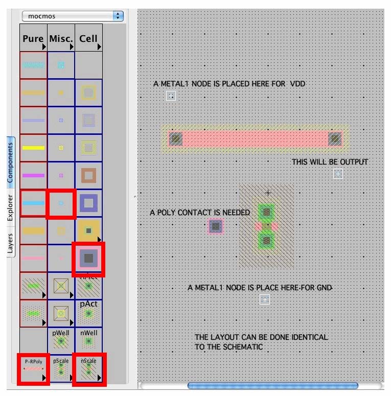
The objects to select in the layout menu are basically the same objects as
in the schematic menu, but they are just in layout format. For instance a
resistor and a transistor can be place just like in the schematic.
But the transistor needs an additional gate contact to be placed.
The power, ground, and output nodes involve placing METAL1 pins in the
same locations.
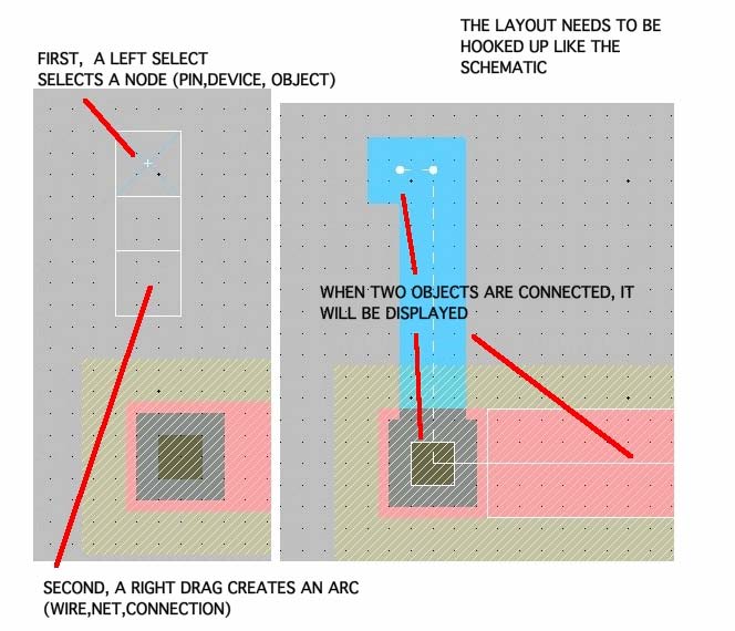
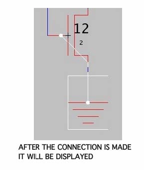
The top METAL1 pin will be the vdd pin. In ELECTRIC, this pin (a node) , needs
to be connected the resistor (another node) using an arc (or wire). This is done
just like in the schematic. The object is first left mouse selected. An arc
is then right mouse dragged from the pin to the resistor. When the connection is
made, it will be displayed.
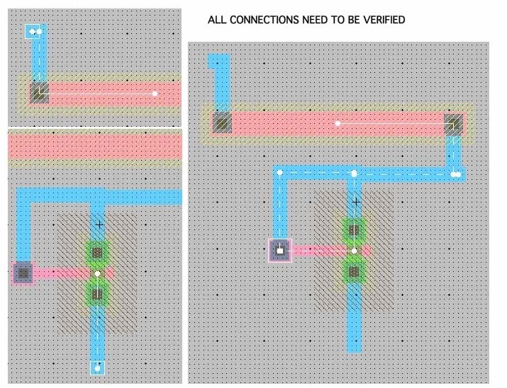
It is very easy for something to look like it is connected when it really is not.
So every object (node) needs to be verified that it is correctly connected
with all the other nodes.
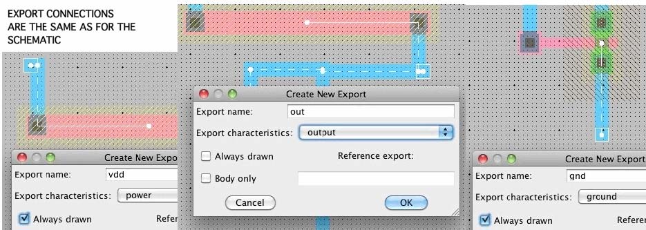
The exports (net labels) are all done the same way as in the schematic.
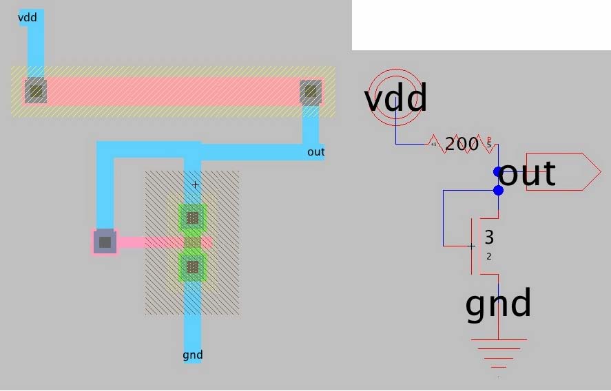
Now the layout is pretty much the same as the schematic.
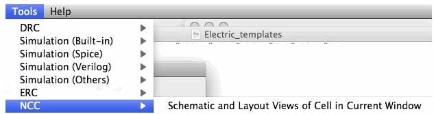
Run a NCC, and except for size, everything will match.
=================================60=================================
Hierarchical NCC every cell in the design: cell 'diode{sch}' cell 'diode{lay}'
Comparing: diode:diode{sch} with: diode:diode{lay}
exports match, topologies match, sizes not checked in 0.304 seconds.
Summary for all cells: exports match, topologies match, sizes not checked
NCC command completed in: 0.312 seconds.
NCC by default does not check sizes.
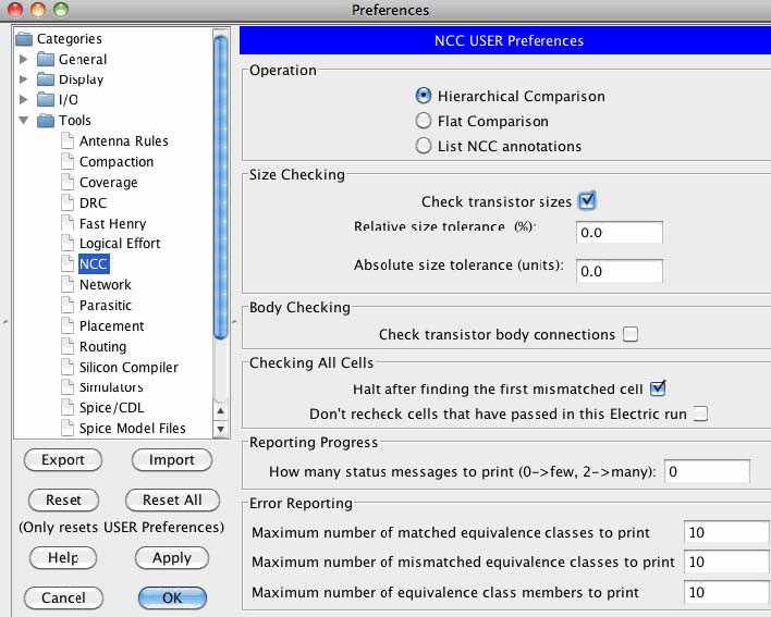
Check transistor sizes needs to be selected in the preference dialog.
Run NCC again and these are all the errors.
Hierarchical NCC every cell in the design: cell 'diode{sch}' cell 'diode{lay}'
Comparing: diode:diode{sch} with: diode:diode{lay}
There are 3 size mismatches.
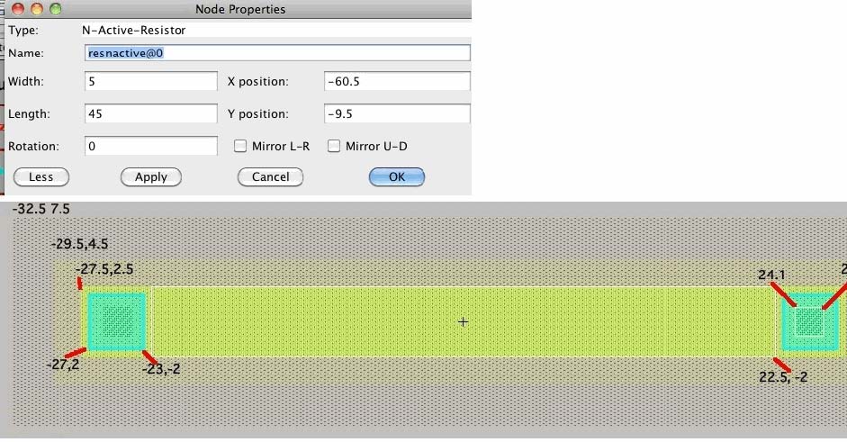
resppoly lengths don't match. relativeError=2150.0% absoluteError=43.0
L=2.0 for resppoly resppoly@0 in Cell: diode:diode{sch} W= 2.0 L=2.0 S= vdd E= out
L=45.0 for resppoly resppoly@0 in Cell: diode:diode{lay} W= 5.0 L=45.0 S= vdd E= out
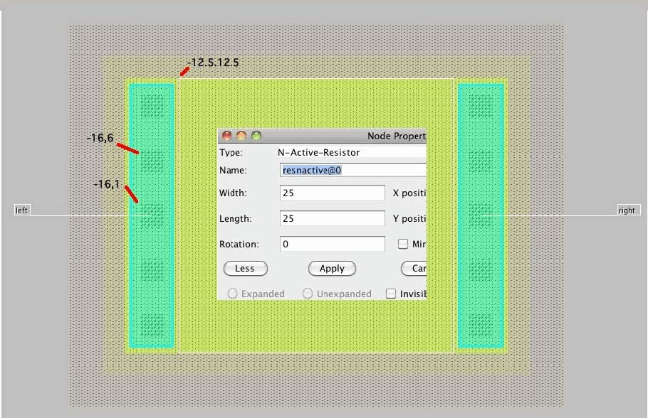
nmos widths don't match. relativeError=300.0% absoluteError=9.0
W=3.0 for nmos nmos@1 in Cell: diode:diode{lay} W=3.0 L=2.0 S=out G=out D=gnd
W=12.0 for nmos nmos@0 in Cell: diode:diode{sch} W=12.0 L=2.0 S=gnd G=out D=out
resppoly widths don't match. relativeError=150.0% absoluteError=3.0
W=2.0 for resppoly resppoly@0 in Cell: diode:diode{sch} W= 2.0 L=2.0 S= vdd E= out
W=5.0 for resppoly resppoly@0 in Cell: diode:diode{lay} W= 5.0 L=45.0 S= vdd E= out
exports match, topologies match, sizes mismatch in 0.0040 seconds.
The node size mismatches can be seen by double clicking the same nodes
(or objects) in both the layout and schematic "views".
=================================67=================================
Hierarchical NCC every cell in the design: cell 'diode{sch}' cell 'diode{lay}'
Comparing: diode:diode{sch} with: diode:diode{lay}
exports match, topologies match, sizes match in 0.0010 seconds.
Summary for all cells: exports match, topologies match, sizes match
NCC command completed in: 0.0020 seconds.
Make layout match the schematic, and running NCC will produce the result above. Notice
there is no equations that map the width and length of resistor to a resistor value.
Remember also that the width and length of transistors are in "layout units".
==========================MATCHING_SIZES==========================================
The full "library" file for both layout and schematic "views" for the "diode" cell is
below. Notice that parameters to the transistor and resistor are not listed in the layout
view, like they are in the schematic view. That is because standard size transistors and
resistors are being used in the layout. The missing details to match size are all located inside what is commonly called a "technology file".
It is possible to modify and create a tech file, and add it to ELECTRIC. For the moment,
the external tech file "tech6.xml" has not been used.
# header information:
Hdiode|9.04
# Views:
Vlayout|lay
Vschematic|sch
# Tools:
Ouser|SoftTechnologies()S/Users/don_sauer/Downloads/stabie/CAD/tech6.xml
# Technologies:
Tmocmos|mocmosAnalog()BT
# Cell diode;1{lay}
Cdiode;1{lay}||mocmos|1401999649677|1402002627997|
Ngeneric:Facet-Center|art@0||0|0||||AV
NMetal-1-Polysilicon-1-Con|contact@0||-16.5|-10.5||||
NN-Transistor-Scalable|nmos@1||-0.5|-10.5||||
NMetal-1-Pin|pin@0||-30.5|30.5||||
NMetal-1-Pin|pin@1||22|6||||
NMetal-1-Pin|pin@3||-29|30.5||||
NMetal-1-Pin|pin@4||21|6||||
NMetal-1-Pin|pin@5||-0.5|6.5||||
NMetal-1-Pin|pin@6||-0.5|6||||
NMetal-1-Pin|pin@11||-0.5|-31||||
NMetal-1-Pin|pin@12||-16.5|6.5||||
NP-Poly-Resistor|resppoly@0||-4|17||||
AMetal-1|net@0|||S1800|pin@0||-30.5|30.5|pin@3||-29|30.5
AMetal-1|net@1|||S2700|resppoly@0|left|-29|17|pin@3||-29|30.5
AMetal-1|net@2|||S0|pin@1||22|6|pin@4||21|6
AMetal-1|net@3|||S900|resppoly@0|right|21|17|pin@4||21|6
AMetal-1|net@4|||S900|resppoly@0|right|21|17|pin@4||21|6
AMetal-1|net@5|||S2700|nmos@1|diff-top|-0.5|-6|pin@5||-0.5|6.5
AMetal-1|net@6|||S900|pin@5||-0.5|6.5|pin@6||-0.5|6
AMetal-1|net@7|||S0|pin@1||22|6|pin@6||-0.5|6
APolysilicon-1|net@8|||S0|nmos@1|poly-left|-4|-10.5|contact@0||-16.5|-10.5
AMetal-1|net@15|||S2700|pin@11||-0.5|-31|nmos@1|diff-bottom|-0.5|-15
AMetal-1|net@16|||S|nmos@1|diff-bottom|-0.5|-15|nmos@1|diff-bottom|-0.5|-15
AMetal-1|net@17|||S0|pin@5||-0.5|6.5|pin@12||-16.5|6.5
AMetal-1|net@18|||S900|pin@12||-16.5|6.5|contact@0||-16.5|-10.5
Egnd||D5G2;|pin@11||G/A
Eout||D5G2;|pin@1||O/A
Evdd||D5G2;|pin@0||P/A
X
# Cell diode;1{sch}
Cdiode;1{sch}||schematic|1401995523765|1402003689926|
Ngeneric:Facet-Center|art@0||0|0||||AV
NOff-Page|conn@0||5|4||||
NGround|gnd@0||1.5|-5||||
NTransistor|nmos@0||-0.5|0|||R||ATTR_length(D5G0.5;X-0.5;Y-1;)S2|ATTR_width(D5G1;X0.5;Y-1;)S3
NWire_Pin|pin@0||-1.5|3||||
NWire_Pin|pin@1||1.5|3||||
NWire_Pin|pin@2||1.5|4||||
NWire_Pin|pin@3||-4|5.5||||
NPower|pwr@0||-4|8||||
NResistor|resppoly@0||-0.5|5.5||||2|ATTR_length(D5G0.25;X-1.5;)D45.0|ATTR_width(D5G0.5;X1.5;)D5.0|SCHEM_resistance(D5G1;)S200
Awire|net@1|||900|nmos@0|s|1.5|-2|gnd@0||1.5|-3
Awire|net@3|||2700|nmos@0|g|-1.5|0|pin@0||-1.5|3
Awire|net@4|||2700|nmos@0|d|1.5|2|pin@1||1.5|3
Awire|net@6|||1800|pin@0||-1.5|3|pin@1||1.5|3
Awire|net@7|||2700|pin@1||1.5|3|pin@2||1.5|4
Awire|net@8|||2700|pin@2||1.5|4|resppoly@0|b|1.5|5.5
Awire|net@9|||0|conn@0|a|3|4|pin@2||1.5|4
Awire|net@10|||0|resppoly@0|a|-2.5|5.5|pin@3||-4|5.5
Awire|net@11|||2700|pin@3||-4|5.5|pwr@0||-4|8
Egnd||D5G2;|gnd@0||G/A
Eout||D5G2;|conn@0|a|O/A
Evdd||D5G2;|pwr@0||P/A
X
The cell is defined as Cdiode. The "C" in front denotes a cell. The layout view includes
the tech file's process name (moscmos) which contain most of the dimension information.
==========================TECH_FILE_TEMPLATES=================================
Most critical details exist within the technology file. The tech file is
an area where spending time will save a great deal of time. The best way to
understand the tech file is to see how all it's information maps to what gets
displayed in the layout window.
An external technology file can be added as is shown above. If there is and
error in the file, it will not load. If the file loads OK, it is available
for selection form the menu.
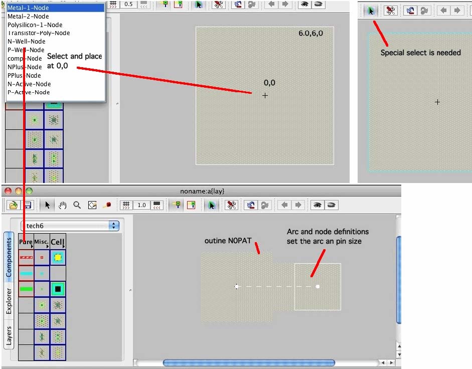
The tech file needs the following.
1) Header (for things like scale values)
2) Layer definitions
3) Arc definitions
4) Node definitions
5) Menu definitions
6) GDSII definitions
7) DRC definitions
The following is not a tech file, but rather an attempt to show how the
format of the tech file maps to what gets displayed.
=======================TECH_FILE_Header=================================
<technology name="tech6"
xmlns="http://electric.sun.com/Technology"
xmlns:xsi="http://www.w3.org/2001/XMLSchema-instance"
xsi:schemaLocation="http://electric.sun.com/Technology ../../technology/Technology.xsd">
<shortName>tech6</shortName>
<description></description>
<numMetals min="2" max="2" default="2"/>
<scale value="100.0" relevant="true"/>
<resolution value="0.0"/>
<defaultFoundry value="NONE"/>
<minResistance value="1.0"/>
<minCapacitance value="0.1"/>
<!-- Transparent layers -->
<transparentLayer transparent="1"><r>96</r><g>209</g><b>255</b></transparentLayer>
<transparentLayer transparent="2"><r>255</r><g>155</g><b>192</b></transparentLayer>
<transparentLayer transparent="3"><r>107</r><g>226</g><b>96</b></transparentLayer>
<transparentLayer transparent="4"><r>224</r><g>95</g><b>255</b></transparentLayer>
<transparentLayer transparent="5"><r>247</r><g>251</g><b>20</b></transparentLayer>
<transparentLayer transparent="6"><r>255</r><g>25</g><b>20</b></transparentLayer>
<transparentLayer transparent="7"><r>25</r><g>255</g><b>20</b></transparentLayer>
<transparentLayer transparent="8"><r>255</r><g>255</g><b>20</b></transparentLayer>
The first part of the tech file provides the scale value which in this case says
that one layout unit corresponds to 100 nanometers.
======================LAYERS_DEFINITIONS=================================
<layer name="Metal-1" fun="METAL1"><opaqueColor r="10" g="250" b="250"/>
<patternedOnDisplay>true</patternedOnDisplay><patternedOnPrinter>true</patternedOnPrinter>
<pattern>X X X X X X X X </pattern>
<pattern> X X X X X X X X</pattern>
<pattern>X X X X X X X X </pattern>
<pattern> X X X X X X X X</pattern>
<pattern>X X X X X X X X </pattern>
<pattern> X X X X X X X X</pattern>
<pattern>X X X X X X X X </pattern>
<pattern> X X X X X X X X</pattern>
<pattern>X X X X X X X X </pattern>
<pattern> X X X X X X X X</pattern>
<pattern>X X X X X X X X </pattern>
<pattern> X X X X X X X X</pattern>
<pattern>X X X X X X X X </pattern>
<pattern> X X X X X X X X</pattern>
<pattern>X X X X X X X X </pattern>
<pattern> X X X X X X X X</pattern>
<outlined>PAT_T1</outlined><opacity>0.9</opacity><foreground>true</foreground>
<display3D thick="2.65" height="16.5" mode="NONE" factor="0.2"/>
<cifLayer cif="CMF"/><skillLayer skill="metal1"/>
<parasitics resistance="0.078" capacitance="0.1209" edgeCapacitance="0.1104"/>
<pureLayerNode name="Metal-1-Node" port="metal-1"><lambda>3.0</lambda>
<portArc>Metal-1</portArc></pureLayerNode>
</layer>
This layer definition defines layer "Metal-1" to have a pattern, a special color,
and a special outline. This layer will have a Port, a Pin, and Arc, and a Node
associated with it.
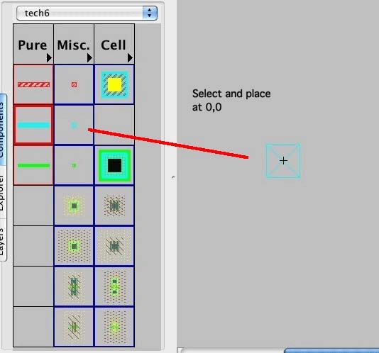
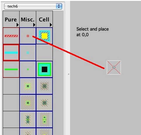
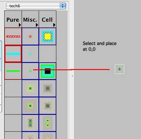
The layout window has a special menu location labeled "PURE" at the
upper left corner of the menu. The terms pureLayerNode name="Metal-1-Node"
define what goes there. The port="metal-1" is defined in the
primitiveNode definitions. The lambda 3.0 says that it will be drawn in 3 units.
The portArc Metal-1 refers to the arcProto definitions in which lambda 1.5
draws 1.5 units on both sides of a arc path.
The layer definition refers to both Arc and Node definitions, which are listed below
only for information sake. ELECTRIC has problems if the layer, arc, and
node definitions are grouped together.
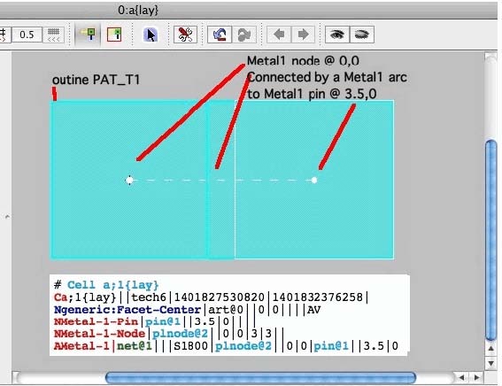
<primitiveNode name="Metal-1-Pin" fun="PIN">
<shrinkArcs/><diskOffset untilVersion="2" x="1.5" y="1.5"/>
<nodeBase><box><lambdaBox klx="-1.5" khx="1.5" kly="-1.5" khy="1.5"/></box></nodeBase>
<nodeLayer layer="Metal-1" style="CROSSED"><box><lambdaBox klx="-1.5" khx="1.5" kly="-1.5" khy="1.5"/>
</box></nodeLayer>
<primitivePort name="metal-1">
<portAngle primary="0" range="180"/><portTopology>0</portTopology>
<box><lambdaBox klx="0.0" khx="0.0" kly="0.0" khy="0.0"/></box>
<portArc>Metal-1</portArc>
</primitivePort>
</primitiveNode>
<arcProto name="Metal-1" fun="METAL1">
<wipable/><extended>true</extended>
<fixedAngle>true</fixedAngle><angleIncrement>90</angleIncrement>
<antennaRatio>400.0</antennaRatio><diskOffset untilVersion="2" width="1.5"/>
<arcLayer layer="Metal-1" style="FILLED"><lambda>1.5</lambda></arcLayer>
</arcProto>
The layer, arc, and node definitions define Metal-1 to always be drawn at 3 units.
This means that DRC rules are automatically being
written into the tech file.
<layer name="Metal-2" fun="METAL2"><transparentColor transparent="6"/>
<patternedOnDisplay>true</patternedOnDisplay><patternedOnPrinter>true</patternedOnPrinter>
<pattern> XXXX XXXX </pattern>
<pattern> XXXX XXXX </pattern>
<pattern> XXXX XXXX </pattern>
<pattern>XXXX XXXX </pattern>
<pattern>XXX XXXX X</pattern>
<pattern> XXXX XX</pattern>
<pattern> XXXX XXX</pattern>
<pattern> XXXX XXXX</pattern>
<pattern> XXXX XXXX </pattern>
<pattern> XXXX XXXX </pattern>
<pattern> XXXX XXXX </pattern>
<pattern>XXXX XXXX </pattern>
<pattern>XXX XXXX X</pattern>
<pattern> XXXX XX</pattern>
<pattern> XXXX XXX</pattern>
<pattern> XXXX XXXX</pattern>
<outlined>PAT_S</outlined><opacity>0.7</opacity><foreground>true</foreground>
<display3D thick="2.65" height="22.15" mode="NONE" factor="0.2"/>
<cifLayer cif="CMS"/><skillLayer skill="metal2"/>
<parasitics resistance="0.078" capacitance="0.0843" edgeCapacitance="0.0974"/>
<pureLayerNode name="Metal-2-Node" port="metal-2"><lambda>3.0</lambda>
<portArc>Metal-2</portArc></pureLayerNode>
</layer>
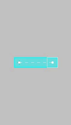
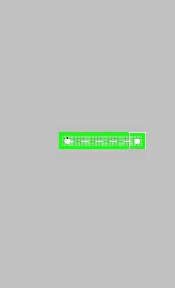
The mapping to the display of Metal2 is shown above. In this example, a Metal2 node
is first placed at 0,0. It is left mouse selected. It is then right mouse dragged
to 0,4.5 and released. This will create both a Metal2 pin at 0,4.5 and a Metal2 arc
between the two points. This all can be seen in the saved file.
<layer name="Polysilicon-1" fun="POLY1"><transparentColor transparent="7"/>
<patternedOnDisplay>true</patternedOnDisplay><patternedOnPrinter>true</patternedOnPrinter>
<pattern> X X X X</pattern>
<pattern>XXXXXXXXXXXXXXXX</pattern>
<pattern> X X X X</pattern>
<pattern> X X X X X X X X</pattern>
<pattern> X X X X</pattern>
<pattern>XXXXXXXXXXXXXXXX</pattern>
<pattern> X X X X</pattern>
<pattern> X X X X X X X X</pattern>
<pattern> X X X X</pattern>
<pattern>XXXXXXXXXXXXXXXX</pattern>
<pattern> X X X X</pattern>
<pattern> X X X X X X X X</pattern>
<pattern> X X X X</pattern>
<pattern>XXXXXXXXXXXXXXXX</pattern>
<pattern> X X X X</pattern>
<pattern> X X X X X X X X</pattern>
<outlined>PAT_T2</outlined><opacity>1.0</opacity><foreground>true</foreground>
<display3D thick="1.0" height="13.0" mode="NONE" factor="0.2"/>
<cifLayer cif="CPG"/><skillLayer skill="poly"/>
<parasitics resistance="6.2" capacitance="0.1467" edgeCapacitance="0.0608"/>
<pureLayerNode name="Polysilicon-1-Node" port="polysilicon-1"><lambda>2.0</lambda>
<portArc>Polysilicon-1</portArc>
</pureLayerNode>
</layer>
A new pattern, new outline, and new lambda is being tried out above.
<layer name="N-Well" fun="WELLN"><opaqueColor r="255" g="255" b="20"/>
<patternedOnDisplay>true</patternedOnDisplay><patternedOnPrinter>true</patternedOnPrinter>
<pattern> X X </pattern>
<pattern> </pattern>
<pattern> X X </pattern>
<pattern> </pattern>
<pattern> X X </pattern>
<pattern> </pattern>
<pattern> X X </pattern>
<pattern> </pattern>
<pattern> X X </pattern>
<pattern> </pattern>
<pattern> X X </pattern>
<pattern> </pattern>
<pattern> X X </pattern>
<pattern> </pattern>
<pattern> X X </pattern>
<pattern> </pattern>
<outlined>NOPAT</outlined><opacity>1.0</opacity><foreground>false</foreground>
<display3D thick="13.0" height="0.0" mode="NICEST" factor="0.8"/>
<cifLayer cif="CWN"/><skillLayer skill="nwell"/>
<pureLayerNode name="N-Well-Node" port="well"><lambda>12.0</lambda>
<portArc>N-Well</portArc>
</pureLayerNode>
</layer>
This example demonstrates how the arc, node and pin definitions are made
in three different locations within the tech file. A manual effort is required
to be consistent.
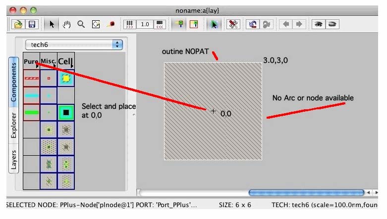
<layer name="PPlus" fun="IMPLANTP"><opaqueColor r="139" g="99" b="46"/>
<patternedOnDisplay>true</patternedOnDisplay><patternedOnPrinter>true</patternedOnPrinter>
<pattern> X X </pattern>
<pattern> X X</pattern>
<pattern>X X </pattern>
<pattern> X X </pattern>
<pattern> X X </pattern>
<pattern> X X </pattern>
<pattern> X X </pattern>
<pattern> X X </pattern>
<pattern> X X </pattern>
<pattern> X X</pattern>
<pattern>X X </pattern>
<pattern> X X </pattern>
<pattern> X X </pattern>
<pattern> X X </pattern>
<pattern> X X </pattern>
<pattern> X X </pattern>
<outlined>NOPAT</outlined><opacity>1.0</opacity><foreground>true</foreground>
<display3D thick="1.0" height="1.0" mode="NONE" factor="1.0"/><cifLayer cif="Not set"/>
<skillLayer skill="PPlus"/><parasitics resistance="1.0" capacitance="0.0" edgeCapacitance="0.0"/>
<pureLayerNode name="PPlus-Node" port="Port_PPlus"><lambda>6.0</lambda></pureLayerNode>
</layer>
Sometimes a layer is needed that is not connected to anything. Notice that this
layer has no Arc definition.
<layer name="N-Active" fun="DIFFN"><opaqueColor r="200" g="255" b="46"/>
<patternedOnDisplay>true</patternedOnDisplay><patternedOnPrinter>true</patternedOnPrinter>
<pattern>X X X X X X X X </pattern>
<pattern>X X X X X X X X </pattern>
<pattern>X X X X X X X X </pattern>
<pattern>X X X X X X X X </pattern>
<pattern>X X X X X X X X </pattern>
<pattern>X X X X X X X X </pattern>
<pattern>X X X X X X X X </pattern>
<pattern>X X X X X X X X </pattern>
<pattern>X X X X X X X X </pattern>
<pattern>X X X X X X X X </pattern>
<pattern>X X X X X X X X </pattern>
<pattern>X X X X X X X X </pattern>
<pattern>X X X X X X X X </pattern>
<pattern>X X X X X X X X </pattern>
<pattern>X X X X X X X X </pattern>
<pattern>X X X X X X X X </pattern>
<outlined>NOPAT</outlined><opacity>1.0</opacity><foreground>true</foreground>
<display3D thick="4.0" height="9.0" mode="NONE" factor="0.0"/>
<cifLayer cif="CAA"/><skillLayer skill="aa"/>
<parasitics resistance="3.0" capacitance="0.9" edgeCapacitance="0.0"/>
<pureLayerNode name="N-Active-Node" port="active"><lambda>3.0</lambda>
<portArc>N-Active</portArc></pureLayerNode>
</layer>
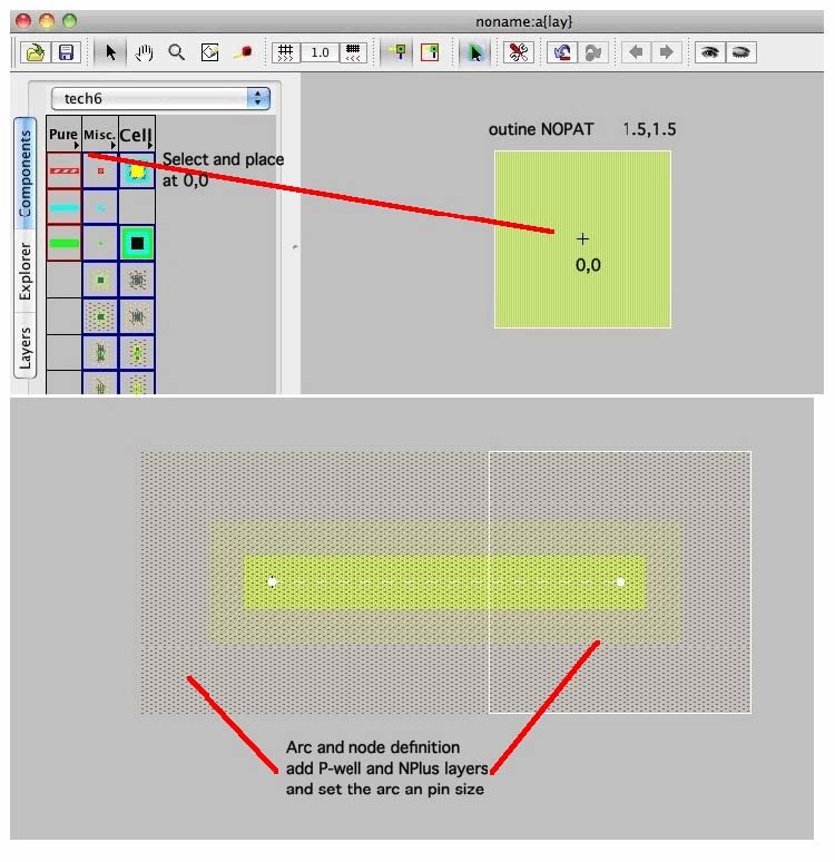
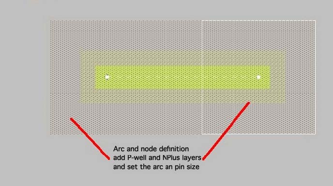
Layers are often required to be within other layers by some minimum amount.
That is why DRC rules have a set of surround rules. ELECTRIC can make it
where adding a layer automatically includes the surrounding layers. The
arc and node definitions provided for reference sake below show how this is
done. Installing and dragging a Nactive pin will create three layers all
having the right enclosure. Remember the layer, arc and node definitions have
trouble being grouped together.
<arcProto name="N-Active" fun="DIFFN">
<wipable/><extended>true</extended>
<fixedAngle>true</fixedAngle><angleIncrement>90</angleIncrement>
<antennaRatio>200.0</antennaRatio><diskOffset untilVersion="1" width="7.5"/><diskOffset untilVersion="2" width="1.5"/>
<arcLayer layer="N-Active" style="FILLED"><lambda>1.5</lambda></arcLayer>
<arcLayer layer="P-Well" style="FILLED"><lambda>7.5</lambda></arcLayer>
<arcLayer layer="NPlus" style="FILLED"><lambda>3.5</lambda></arcLayer>
</arcProto>
<primitiveNode name="N-Active-Pin" fun="PIN">
<shrinkArcs/><diskOffset untilVersion="1" x="7.5" y="7.5"/><diskOffset untilVersion="2" x="1.5" y="1.5"/>
<nodeBase><box><lambdaBox klx="-7.5" khx="7.5" kly="-7.5" khy="7.5"/></box></nodeBase>
<nodeLayer layer="N-Active" style="CROSSED"><box><lambdaBox klx="-1.5" khx="1.5" kly="-1.5" khy="1.5"/></box></nodeLayer>
<nodeLayer layer="P-Well" style="CROSSED"><box><lambdaBox klx="-7.5" khx="7.5" kly="-7.5" khy="7.5"/></box></nodeLayer>
<nodeLayer layer="NPlus" style="CROSSED"><box><lambdaBox klx="-3.5" khx="3.5" kly="-3.5" khy="3.5"/></box></nodeLayer>
<primitivePort name="n-active">
<portAngle primary="0" range="180"/><portTopology>0</portTopology>
<box><lambdaBox klx="0.0" khx="0.0" kly="0.0" khy="0.0"/></box>
<portArc>N-Active</portArc>
</primitivePort>
</primitiveNode>
=======================ARC_DEFINITIONS====================================
ELECTRIC seems to like to have arc definitons grouped together.
<arcProto name="Metal-1" fun="METAL1">
<wipable/><extended>true</extended>
<fixedAngle>true</fixedAngle><angleIncrement>90</angleIncrement>
<antennaRatio>400.0</antennaRatio><diskOffset untilVersion="2" width="1.5"/>
<arcLayer layer="Metal-1" style="FILLED"><lambda>1.5</lambda></arcLayer>
</arcProto>
For the arc, lambda seems to be the distance on either side of a path
which is connecting two nodes. In this case 1.5 is added on each side of
the path tocreate a metal-1 trace that is 3 units wide.
<arcProto name="N-Active" fun="DIFFN">
<wipable/><extended>true</extended>
<fixedAngle>true</fixedAngle><angleIncrement>90</angleIncrement>
<antennaRatio>200.0</antennaRatio><diskOffset untilVersion="1" width="7.5"/><diskOffset untilVersion="2" width="1.5"/>
<arcLayer layer="N-Active" style="FILLED"><lambda>1.5</lambda></arcLayer>
<arcLayer layer="P-Well" style="FILLED"><lambda>7.5</lambda></arcLayer>
<arcLayer layer="NPlus" style="FILLED"><lambda>3.5</lambda></arcLayer>
</arcProto>
The node definition for N-Active automatically surrounds a pin with all the needed
layers. Dragging an arc will create another pin. The path connecting the two nodes
should be defined to include all the needed surrounding layers.
==========================NODE_DEFINITIONS==============================
<primitiveNode name="Metal-1-Pin" fun="PIN">
<shrinkArcs/><diskOffset untilVersion="2" x="1.5" y="1.5"/>
<nodeBase><box><lambdaBox klx="-1.5" khx="1.5" kly="-1.5" khy="1.5"/></box></nodeBase>
<nodeLayer layer="Metal-1" style="CROSSED"><box><lambdaBox klx="-1.5" khx="1.5" kly="-1.5" khy="1.5"/></box></nodeLayer>
<primitivePort name="metal-1">
<portAngle primary="0" range="180"/><portTopology>0</portTopology>
<box><lambdaBox klx="0.0" khx="0.0" kly="0.0" khy="0.0"/></box>
<portArc>Metal-1</portArc>
</primitivePort>
</primitiveNode>
This appears to be the place where a node in the menu for metal-1 gets defined as
a cross. Notice that a drag will turn the cross into a filled metal-1 bar having
two nodes connected by an arc.
<primitiveNode name="Metal-2-Pin" fun="PIN">
<shrinkArcs/><diskOffset untilVersion="2" x="1.5" y="1.5"/>
<nodeBase><box><lambdaBox klx="-1.5" khx="1.5" kly="-1.5" khy="1.5"/></box></nodeBase>
<nodeLayer layer="Metal-2" style="CROSSED"><box><lambdaBox klx="-1.5" khx="1.5" kly="-1.5" khy="1.5"/></box></nodeLayer>
<primitivePort name="metal-2">
<portAngle primary="0" range="180"/><portTopology>0</portTopology>
<box><lambdaBox klx="0.0" khx="0.0" kly="0.0" khy="0.0"/></box>
<portArc>Metal-2</portArc>
</primitivePort>
</primitiveNode>
Putting a metal-2 trace, metal-2 pin, and a metal-2 to metal-1 connection together
in the menu seems to come natural.
<primitiveNode name="Polysilicon-1-Pin" fun="PIN">
<shrinkArcs/><diskOffset untilVersion="2" x="1.0" y="1.0"/>
<nodeBase><box><lambdaBox klx="-1.0" khx="1.0" kly="-1.0" khy="1.0"/></box></nodeBase>
<nodeLayer layer="Polysilicon-1" style="CROSSED"><box><lambdaBox klx="-1.0" khx="1.0" kly="-1.0" khy="1.0"/>
</box></nodeLayer>
<primitivePort name="polysilicon-1">
<portAngle primary="0" range="180"/><portTopology>0</portTopology>
<box><lambdaBox klx="0.0" khx="0.0" kly="0.0" khy="0.0"/></box>
<portArc>Polysilicon-1</portArc>
</primitivePort>
</primitiveNode>
Transistors seem to work best if the gate is added manually. So putting a poly trace,
a poly pin, and a poly to metal-1 connection together in the menu seems to work best.
<primitiveNode name="N-Well-Pin" fun="PIN">
<shrinkArcs/><diskOffset untilVersion="2" x="1.5" y="1.5"/>
<nodeBase><box><lambdaBox klx="-4.0" khx="4.0" kly="-4.0" khy="4.0"/></box></nodeBase>
<nodeLayer layer="N-Well" style="CROSSED"><box><lambdaBox klx="-4.0" khx="4.0" kly="-4.0" khy="4.0"/></box></nodeLayer>
<primitivePort name="n-active">
<portAngle primary="0" range="180"/><portTopology>0</portTopology>
<box><lambdaBox klx="0.0" khx="0.0" kly="0.0" khy="0.0"/></box>
<portArc>N-Well</portArc>
</primitivePort>
</primitiveNode>
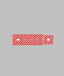
This Nwell cell is added to demonstrate how the tech file automatically includes DRC.
The layer, arc, and node definitions are inclined to draw everything at what
you would expect to be a minimum width. After a geometry has been drawn,
a node can be double clicked to manually reduce its
width to demonstrate DRC working
<primitiveNode name="N-Active-Pin" fun="PIN">
<shrinkArcs/><diskOffset untilVersion="1" x="7.5" y="7.5"/><diskOffset untilVersion="2" x="1.5" y="1.5"/>
<nodeBase><box><lambdaBox klx="-7.5" khx="7.5" kly="-7.5" khy="7.5"/></box></nodeBase>
<nodeLayer layer="N-Active" style="CROSSED"><box><lambdaBox klx="-1.5" khx="1.5" kly="-1.5" khy="1.5"/></box></nodeLayer>
<nodeLayer layer="P-Well" style="CROSSED"><box><lambdaBox klx="-7.5" khx="7.5" kly="-7.5" khy="7.5"/></box></nodeLayer>
<nodeLayer layer="NPlus" style="CROSSED"><box><lambdaBox klx="-3.5" khx="3.5" kly="-3.5" khy="3.5"/></box></nodeLayer>
<primitivePort name="n-active">
<portAngle primary="0" range="180"/><portTopology>0</portTopology>
<box><lambdaBox klx="0.0" khx="0.0" kly="0.0" khy="0.0"/></box>
<portArc>N-Active</portArc>
</primitivePort>
</primitiveNode>
The arc and node definitions are written such that selecting a node layer
will always include the layers that need to surround that layer with
the proper DRC spacings.
<primitiveNode name="Metal-1-Metal-2-Con" fun="CONTACT">
<diskOffset untilVersion="1" x="2.5" y="2.5"/><diskOffset untilVersion="2" x="2.0" y="2.0"/>
<nodeBase><box><lambdaBox klx="-2.0" khx="2.0" kly="-2.0" khy="2.0"/></box></nodeBase>
<nodeLayer layer="Metal-1" style="FILLED"><box><lambdaBox klx="-2.0" khx="2.0" kly="-2.0" khy="2.0"/></box></nodeLayer>
<nodeLayer layer="Metal-2" style="FILLED"><box><lambdaBox klx="-2.0" khx="2.0" kly="-2.0" khy="2.0"/></box></nodeLayer>
<nodeLayer layer="Via1" style="FILLED">
<multicutbox sizex="2.0" sizey="2.0" sep1d="3.0" sep2d="3.0">
<lambdaBox klx="0.0" khx="0.0" kly="0.0" khy="0.0"/></multicutbox></nodeLayer>
<primitivePort name="metal-1-metal-2">
<portAngle primary="0" range="180"/><portTopology>0</portTopology>
<box><lambdaBox klx="-1.0" khx="1.0" kly="-1.0" khy="1.0"/></box>
<portArc>Metal-1</portArc>
<portArc>Metal-2</portArc>
</primitivePort>
<minSizeRule width="5.0" height="5.0" rule="8.3, 9.3"/>
</primitiveNode>
The metal-2 to metal-2 contact node definition includes some additional DRC rules,
and some multi portArc definitions. The via layer needs to be a 2x2 square that
is inclosed in both metal-1 and metal-2. But when the X size of the node increases to 14,
the 2x2 via contacts need to be generated 3 units apart. This node has two ports.
It can be connected through using either metal1 or metal2.
Since the layers are always added with the proper DRC enclosure, can the DRC
enclose rule detect any errors?
<primitiveNode name="Metal-1-Polysilicon-1-Con" fun="CONTACT">
<diskOffset untilVersion="2" x="2.5" y="2.5"/>
<nodeBase><box><lambdaBox klx="-2.5" khx="2.5" kly="-2.5" khy="2.5"/></box></nodeBase>
<nodeLayer layer="Metal-1" style="FILLED"><box><lambdaBox klx="-2.0" khx="2.0" kly="-2.0" khy="2.0"/>
</box></nodeLayer>
<nodeLayer layer="Polysilicon-1" style="FILLED"><box><lambdaBox klx="-2.5" khx="2.5" kly="-2.5" khy="2.5"/>
</box></nodeLayer>
<nodeLayer layer="Contact" style="FILLED">
<multicutbox sizex="2.0" sizey="2.0" sep1d="3.0" sep2d="3.0">
<lambdaBox klx="0.0" khx="0.0" kly="0.0" khy="0.0"/>
</multicutbox></nodeLayer>
<primitivePort name="metal-1-polysilicon-1">
<portAngle primary="0" range="180"/><portTopology>0</portTopology>
<box><lambdaBox klx="-0.5" khx="0.5" kly="-0.5" khy="0.5"/></box>
<portArc>Polysilicon-1</portArc>
<portArc>Metal-1</portArc>
</primitivePort>
<minSizeRule width="5.0" height="5.0" rule="5.2, 7.3"/>
</primitiveNode>
The metal-1 to poly contact node definition has some spacings that make it easier
to see how the node definitions maps to what is displayed in the layout.
For instance the contacts are 2x2 with a spacing of 3. The metal1 overlap is a
square defined by +/-2.0. The poly overlap is a square defined by +/-2.5.
Notice the that the nodebase is a square defined by +/-2.5.
Notice also that the port is defined to be square defined by +/-0.5.
Any metal-1 or poly arc that gets dragged into that area will make a connection.
<primitiveNode name="Metal-1-N-Well-Con" fun="WELL">
<oldName>Metal-1-Substrate-Con</oldName><diskOffset untilVersion="1" x="8.5" y="8.5"/><diskOffset untilVersion="2" x="2.5" y="2.5"/>
<nodeBase><box><lambdaBox klx="-2.5" khx="2.5" kly="-2.5" khy="2.5"/></box></nodeBase>
<nodeLayer layer="Metal-1" style="FILLED"><box><lambdaBox klx="-2.0" khx="2.0" kly="-2.0" khy="2.0"/></box></nodeLayer>
<nodeLayer layer="N-Active" style="FILLED"><box><lambdaBox klx="-2.5" khx="2.5" kly="-2.5" khy="2.5"/></box></nodeLayer>
<nodeLayer layer="N-Well" style="FILLED"><box><lambdaBox klx="-5.5" khx="5.5" kly="-5.5" khy="5.5"/></box></nodeLayer>
<nodeLayer layer="NPlus" style="FILLED"><box><lambdaBox klx="-4.5" khx="4.5" kly="-4.5" khy="4.5"/></box></nodeLayer>
<nodeLayer layer="Active-Cut" style="FILLED">
<multicutbox sizex="2.0" sizey="2.0" sep1d="3.0" sep2d="3.0"><lambdaBox klx="0.0" khx="0.0" kly="0.0" khy="0.0"/>
</multicutbox></nodeLayer>
<primitivePort name="metal-1-substrate">
<portAngle primary="0" range="180"/><portTopology>0</portTopology>
<box><lambdaBox klx="-0.5" khx="0.5" kly="-0.5" khy="0.5"/></box>
<portArc>Metal-1</portArc>
<portArc>N-Well</portArc>
</primitivePort>
<minSizeRule width="17.0" height="17.0" rule="4.2, 6.2, 7.3"/>
</primitiveNode>
The metal-1 to Nwell contact node definition needs to include several layers with
the correct spacing. In this case the spacing for the layer, the arc, and
the node are not all the same. This is because spacing rules are being included
in the tech file in three different spots.
<primitiveNode name="N-Active-Resistor" fun="RESNACTIVE">
<nodeBase><box><lambdaBox klx="-22.5" khx="22.5" kly="-2.5" khy="2.5"/></box></nodeBase>
<nodeLayer layer="Active-Cut" style="FILLED">
<multicutbox khx="-1.0" sizex="2.0" sizey="2.0" sep1d="3.0" sep2d="3.0">
<lambdaBox klx="-26.0" khx="-24.0" kly="0.0" khy="0.0"/>
</multicutbox></nodeLayer>
<nodeLayer layer="Active-Cut" style="FILLED">
<multicutbox klx="1.0" sizex="2.0" sizey="2.0" sep1d="3.0" sep2d="3.0">
<lambdaBox klx="24.0" khx="26.0" kly="0.0" khy="0.0"/>
</multicutbox></nodeLayer>
<nodeLayer layer="Metal-1" style="FILLED">
<box khx="-1.0"><lambdaBox klx="-27.0" khx="-23.0" kly="-2.0" khy="2.0"/>
</box></nodeLayer>
<nodeLayer layer="Metal-1" style="FILLED" portNum="1">
<box klx="1.0"><lambdaBox klx="23.0" khx="27.0" kly="-2.0" khy="2.0"/>
</box></nodeLayer>
<nodeLayer layer="N-Active" style="FILLED">
<box><lambdaBox klx="-27.5" khx="27.5" kly="-2.5" khy="2.5"/></box></nodeLayer>
<nodeLayer layer="NPlus" style="FILLED">
<box><lambdaBox klx="-29.5" khx="29.5" kly="-4.5" khy="4.5"/></box></nodeLayer>
<nodeLayer layer="P-Well" style="FILLED">
<box><lambdaBox klx="-32.5" khx="32.5" kly="-7.5" khy="7.5"/></box></nodeLayer>
<primitivePort name="left">
<portAngle primary="0" range="180"/>
<portTopology>0</portTopology>
<box khx="-1.0"><lambdaBox klx="-26.0" khx="-24.0" kly="-1.0" khy="1.0"/></box>
<portArc>Metal-1</portArc></primitivePort>
<primitivePort name="right">
<portAngle primary="0" range="180"/>
<portTopology>1</portTopology>
<box klx="1.0"><lambdaBox klx="24.0" khx="26.0" kly="-1.0" khy="1.0"/></box>
<portArc>Metal-1</portArc></primitivePort>
</primitiveNode>
The NPlusR node definition defines the node to be a box that is +/-22.5 x +/-.5. That is
how ELECTRIC thinks of the resistor in terms of size. All the other layers with
their proper overlaps are included as well.
When the resistor is saved in the "library" file, it will not contain all these
spacing dimensions. The resistor is called out having only a location of 0,0.
# Cell onegeo;1{lay}
Conegeo;1{lay}||tech6|1402167301736|1402167376594|
Ngeneric:Facet-Center|art@0||0|0||||AV
NN-Active-Resistor|resnactive@0||0|0||||
X
Double click the resistor, and the dimension can be changed to say 45 x 45. Now
when the resistor is saved, it will contain a -20 adjustment to its length and a
+ 20 adjustment to its width. It is the tech file that defines the default width
and length. Notice there is no reference to the resistance.
# Cell onegeo;1{lay}
Conegeo;1{lay}||tech6|1402167301736|1402167444241|
Ngeneric:Facet-Center|art@0||0|0||||AV
NN-Active-Resistor|resnactive@0||0|0|-20|20||
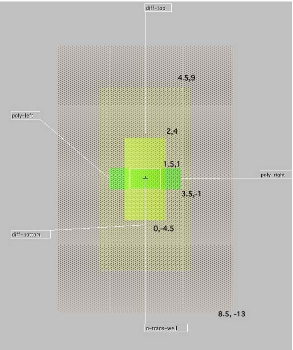
<primitiveNode name="N-Transistor" fun="TRANMOS">
<diskOffset untilVersion="1" x="8.5" y="13.0"/>
<diskOffset untilVersion="2" x="1.5" y="1.0"/>
<nodeBase><box><lambdaBox klx="-1.5" khx="1.5" kly="-1.0" khy="1.0"/></box></nodeBase>
<nodeLayer layer="N-Active" style="FILLED" portNum="1"><box kly="1.0">
<lambdaBox klx="-2.0" khx="2.0" kly="-1.0" khy="4.0"/></box></nodeLayer>
<nodeLayer layer="N-Active" style="FILLED" portNum="3"><box khy="-1.0">
<lambdaBox klx="-2.0" khx="2.0" kly="-4.0" khy="1.0"/></box></nodeLayer>
<nodeLayer layer="N-Active" style="FILLED" portNum="-1"><box>
<lambdaBox klx="-2.0" khx="2.0" kly="-4.0" khy="4.0"/></box></nodeLayer>
<nodeLayer layer="Transistor-Poly" style="FILLED"><box>
<lambdaBox klx="-3.5" khx="3.5" kly="-1.0" khy="1.0"/></box></nodeLayer>
<nodeLayer layer="P-Well" style="FILLED" portNum="-1"><box>
<lambdaBox klx="-8.5" khx="8.5" kly="-13.0" khy="13.0"/></box></nodeLayer>
<nodeLayer layer="NPlus" style="FILLED" portNum="-1"><box>
<lambdaBox klx="-4.5" khx="4.5" kly="-9.0" khy="9.0"/></box></nodeLayer>
<primitivePort name="poly-left">
<portAngle primary="180" range="90"/><portTopology>0</portTopology>
<box klx="0.0" khx="0.0" kly="0.0" khy="0.0"><lambdaBox klx="-3.5" khx="-3.5" kly="0.0" khy="0.0"/></box>
<portArc>Polysilicon-1</portArc></primitivePort>
<primitivePort name="diff-top">
<portAngle primary="90" range="90"/><portTopology>1</portTopology>
<box klx="0.0" khx="0.0" kly="0.0" khy="0.0"><lambdaBox klx="0.0" khx="0.0" kly="4.5" khy="4.5"/></box>
<portArc>N-Active</portArc></primitivePort>
<primitivePort name="poly-right">
<portAngle primary="0" range="90"/><portTopology>0</portTopology>
<box klx="0.0" khx="0.0" kly="0.0" khy="0.0"><lambdaBox klx="3.5" khx="3.5" kly="0.0" khy="0.0"/></box>
<portArc>Polysilicon-1</portArc></primitivePort>
<primitivePort name="diff-bottom">
<portAngle primary="270" range="90"/><portTopology>2</portTopology>
<box klx="0.0" khx="0.0" kly="0.0" khy="0.0"><lambdaBox klx="0.0" khx="0.0" kly="-4.5" khy="-4.5"/></box>
<portArc>N-Active</portArc></primitivePort>
<primitivePort name="n-trans-well">
<portAngle primary="0" range="360"/><portTopology>3</portTopology>
<box klx="0.0" khx="0.0" kly="0.0" khy="0.0"><lambdaBox klx="0.0" khx="0.0" kly="0.0" khy="0.0"/></box>
<portArc>P-Well</portArc></primitivePort>
<minSizeRule width="17.0" height="26.0" rule="2.1, 3.1"/>
</primitiveNode>
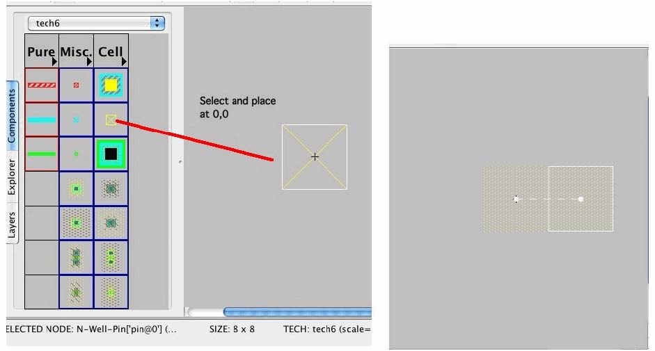
The Export/Show_Ports_on_Node menu will display 5 ports as is shown above. The "poly-left"
or "poly-right" can connect to a poly_contact. The "diff-top" and "diff-bottom" are both
meant to connect to NPlus_activeNodes. The "n-transistor-well" is meant to connect to a Pwell
connection. In this case the nodeBase is incorrectly called out to be a box of +/-1.5 width
and +/- 1.0 length. This is where ELECTRIC thinks the transistor as a "node" exists.
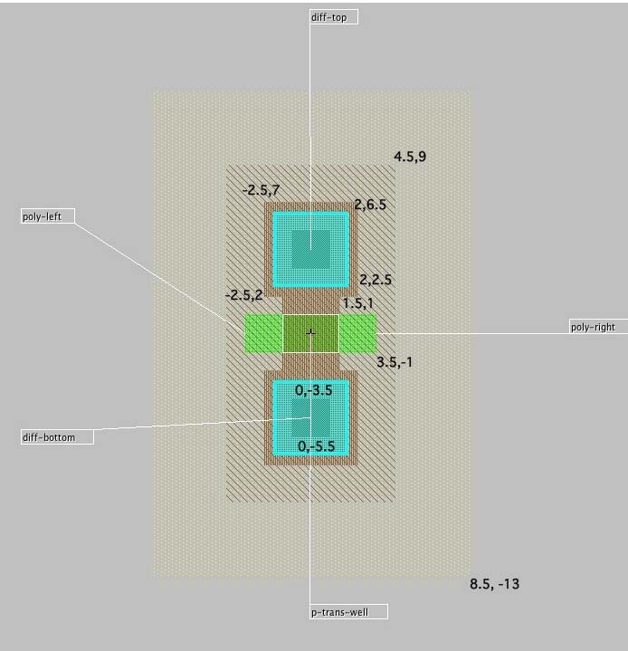
<primitiveNode name="P-Transistor-Scalable" fun="TRAPMOS">
<diskOffset untilVersion="1" x="8.5" y="13.0"/><diskOffset untilVersion="2" x="1.5" y="1.0"/>
<nodeBase><box><lambdaBox klx="-1.5" khx="1.5" kly="-1.0" khy="1.0"/></box></nodeBase>
<nodeLayer layer="P-Active" style="FILLED" portNum="1"><box kly="1.0">
<lambdaBox klx="-2.5" khx="2.5" kly="2.0" khy="7.0"/></box></nodeLayer>
<nodeLayer layer="Metal-1" style="FILLED" portNum="1"><box kly="1.0">
<lambdaBox klx="-2.0" khx="2.0" kly="2.5" khy="6.5"/></box></nodeLayer>
<nodeLayer layer="Active-Cut" style="FILLED" portNum="-1">
<multicutbox kly="1.0" sizex="2.0" sizey="2.0" sep1d="3.0" sep2d="3.0">
<lambdaBox klx="0.0" khx="0.0" kly="4.5" khy="4.5"/>
</multicutbox></nodeLayer>
<nodeLayer layer="P-Active" style="FILLED" portNum="3"><box khy="-1.0">
<lambdaBox klx="-2.5" khx="2.5" kly="-7.0" khy="-2.0"/></box></nodeLayer>
<nodeLayer layer="Metal-1" style="FILLED" portNum="3"><box khy="-1.0">
<lambdaBox klx="-2.0" khx="2.0" kly="-6.5" khy="-2.5"/></box></nodeLayer>
<nodeLayer layer="Active-Cut" style="FILLED" portNum="-1">
<multicutbox khy="-1.0" sizex="2.0" sizey="2.0" sep1d="3.0" sep2d="3.0">
<lambdaBox klx="0.0" khx="0.0" kly="-4.5" khy="-4.5"/>
</multicutbox></nodeLayer>
<nodeLayer layer="P-Active" style="FILLED" portNum="-1"><box>
<lambdaBox klx="-1.5" khx="1.5" kly="-4.0" khy="4.0"/></box></nodeLayer>
<nodeLayer layer="Transistor-Poly" style="FILLED"><box>
<lambdaBox klx="-3.5" khx="3.5" kly="-1.0" khy="1.0"/></box></nodeLayer>
<nodeLayer layer="N-Well" style="FILLED" portNum="-1"><box>
<lambdaBox klx="-8.5" khx="8.5" kly="-13.0" khy="13.0"/></box></nodeLayer>
<nodeLayer layer="PPlus" style="FILLED" portNum="-1"><box>
<lambdaBox klx="-4.5" khx="4.5" kly="-9.0" khy="9.0"/></box></nodeLayer>
<primitivePort name="poly-left">
<portAngle primary="180" range="90"/><portTopology>0</portTopology>
<box klx="0.0" khx="0.0" kly="0.0" khy="0.0"><lambdaBox klx="-3.5" khx="-3.5" kly="0.0" khy="0.0"/></box>
<portArc>Polysilicon-1</portArc></primitivePort>
<primitivePort name="diff-top">
<portAngle primary="90" range="90"/><portTopology>1</portTopology>
<box klx="0.0" khx="0.0" kly="0.0" khy="0.0"><lambdaBox klx="0.0" khx="0.0" kly="4.5" khy="4.5"/></box>
<portArc>P-Active</portArc>
<portArc>Metal-1</portArc></primitivePort>
<primitivePort name="poly-right">
<portAngle primary="0" range="90"/><portTopology>0</portTopology>
<box klx="0.0" khx="0.0" kly="0.0" khy="0.0"><lambdaBox klx="3.5" khx="3.5" kly="0.0" khy="0.0"/></box>
<portArc>Polysilicon-1</portArc></primitivePort>
<primitivePort name="diff-bottom">
<portAngle primary="270" range="90"/><portTopology>2</portTopology>
<box klx="0.0" khx="0.0" kly="0.0" khy="0.0"><lambdaBox klx="0.0" khx="0.0" kly="-4.5" khy="-4.5"/></box>
<portArc>P-Active</portArc>
<portArc>Metal-1</portArc></primitivePort>
<primitivePort name="p-trans-well">
<portAngle primary="0" range="360"/><portTopology>3</portTopology>
<box klx="0.0" khx="0.0" kly="0.0" khy="0.0"><lambdaBox klx="0.0" khx="0.0" kly="0.0" khy="0.0"/></box>
<portArc>N-Well</portArc></primitivePort>
<minSizeRule width="17.0" height="26.0" rule="2.1, 3.1"/>
</primitiveNode>
A more complete and correct version of the PMOS transistor is shown above.
==========================MENU_DEFINITIONS==============================
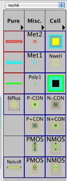
<menuPalette numColumns="3">
<menuBox><menuNodeInst protoName="N-Active-Resistor" function="RESNACTIVE"><menuNodeText text="NplusR"/>
</menuNodeInst></menuBox>
<menuBox><menuNodeInst protoName="P-Transistor" function="TRANMOS"><menuNodeText text="PMOS"/>
</menuNodeInst></menuBox>
<menuBox><menuNodeInst protoName="N-Transistor" function="TRANMOS"><menuNodeText text="NMOS"/>
</menuNodeInst></menuBox>
<menuBox/>
<menuBox><menuNodeInst protoName="P-Transistor-Scalable" function="TRANMOS"><menuNodeText text="PMOS"/>
</menuNodeInst></menuBox>
<menuBox><menuNodeInst protoName="N-Transistor-Scalable" function="TRANMOS"><menuNodeText text="NMOS"/>
</menuNodeInst></menuBox>
<menuBox/>
<menuBox><menuNodeInst protoName="Metal-1-P-Active-Con" function="PIN"><menuNodeText text="P+CON"/>
</menuNodeInst></menuBox>
<menuBox><menuNodeInst protoName="Metal-1-N-Active-Con" function="PIN"><menuNodeText text="N+CON"/>
</menuNodeInst></menuBox>
<menuBox><menuNodeInst protoName="N-Active-Pin" function="PIN"><menuNodeText text="NPlus"/>
</menuNodeInst></menuBox>
<menuBox><menuNodeInst protoName="Metal-1-N-Well-Con" function="PIN"><menuNodeText text="P-CON"/>
</menuNodeInst></menuBox>
<menuBox><menuNodeInst protoName="Metal-1-P-Well-Con" function="PIN"><menuNodeText text="N-CON"/>
</menuNodeInst></menuBox>
<menuBox><menuArc>Polysilicon-1</menuArc></menuBox>
<menuBox><menuNodeInst protoName="Polysilicon-1-Pin" function="PIN"><menuNodeText text="Poly1"/>
</menuNodeInst></menuBox>
<menuBox><menuNodeInst protoName="Metal-1-Polysilicon-1-Con" function="PIN"/></menuBox>
<menuBox><menuArc>Metal-1</menuArc></menuBox>
<menuBox><menuNodeInst protoName="Metal-1-Pin" function="PIN"><menuNodeText text="Met1"/>
</menuNodeInst></menuBox>
<menuBox><menuNodeInst protoName="N-Well-Pin" function="PIN"><menuNodeText text="Nwell"/>
</menuNodeInst></menuBox>
<menuBox><menuArc>Metal-2</menuArc></menuBox>
<menuBox><menuNodeInst protoName="Metal-2-Pin" function="PIN"><menuNodeText text="Met2"/>
</menuNodeInst></menuBox>
<menuBox><menuNode>Metal-1-Metal-2-Con</menuNode></menuBox>
<menuBox><menuText>Pure</menuText></menuBox>
<menuBox><menuText>Misc.</menuText></menuBox>
<menuBox><menuText>Cell</menuText></menuBox>
</menuPalette>
The mapping of the menu definitions are shown above.
==========================GDS_DEFINITIONS==============================
<layerGds layer="N-Well" gds="1"/>
<layerGds layer="N-Active" gds="2"/>
<layerGds layer="P-Well" gds="3"/>
<layerGds layer="Polysilicon-1" gds="4"/>
<layerGds layer="NPlus" gds="5"/>
<layerGds layer="PPlus" gds="6"/>
<layerGds layer="Active-Cut" gds="7"/>
<layerGds layer="Metal-1" gds="8"/>
<layerGds layer="Via1" gds="9"/>
<layerGds layer="Metal-2" gds="10"/>
<layerGds layer="Transistor-Poly" gds="11"/>
<layerGds layer="P-Active" gds="12"/>
<layerGds layer="Poly-Cut" gds="20"/>
<layerGds layer="P-Base" gds="16"/>
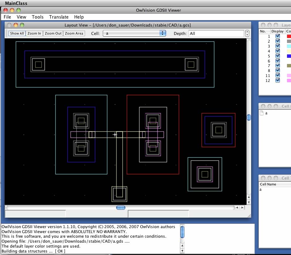
A typical method of exporting the layout is GDSII format. An application like OwlVision
can view whether all the geometries got exported OK. OwlVision can also translate the
GDSII file to text format.
HEADER 3;# version
BGNLIB;
LASTMOD{114-5-41:6:43};# last modification time
LASTACC{114-5-41:8:59};# last access time
LIBNAME a;
UNITS;
USERUNITS 0.0010;
PHYSUNITS 9.999999999999999E-10;
BGNSTR;# Begin of structure
CREATION {114-5-41:6:43};# creation time
LASTMOD{114-5-41:8:59};# last modification time
STRNAME a;
BOUNDARY;
LAYER 11;XY 5;X: -1450;Y: -100;X: -750;Y: -100;X: -750;Y: 100;X: -1450;Y: 100;X: -1450;Y: -100;
LAYER 11;XY 5;X: 900;Y: -100;X: 1600;Y: -100;X: 1600;Y: 100;X: 900;Y: 100;X: 900;Y: -100;
LAYER 6;XY 5;X: 800;Y: -900;X: 1700;Y: -900;X: 1700;Y: 900;X: 800;Y: 900;X: 800;Y: -900;
LAYER 6;XY 5;X: 2500;Y: -1750;X: 3400;Y: -1750;X: 3400;Y: -850;X: 2500;Y: -850;X: 2500;Y: -1750;
LAYER 8;XY 5;X: -50;Y: -2150;X: 350;Y: -2150;X: 350;Y: -1750;X: -50;Y: -1750;X: -50;Y: -2150;
LAYER 8;XY 5;X: -1300;Y: 250;X: -900;Y: 250;X: -900;Y: 650;X: -1300;Y: 650;X: -1300;Y: 250;
LAYER 8;XY 5;X: -1300;Y: -650;X: -900;Y: -650;X: -900;Y: -250;X: -1300;Y: -250;X: -1300;Y: -650;
LAYER 8;XY 5;X: 1050;Y: 250;X: 1450;Y: 250;X: 1450;Y: 650;X: 1050;Y: 650;X: 1050;Y: 250;
LAYER 8;XY 5;X: 1050;Y: -650;X: 1450;Y: -650;X: 1450;Y: -250;X: 1050;Y: -250;X: 1050;Y: -650;
LAYER 8;XY 5;X: -2700;Y: 2100;X: -2300;Y: 2100;X: -2300;Y: 2500;X: -2700;Y: 2500;X: -2700;Y: 2100;
LAYER 8;XY 5;X: 2300;Y: 2100;X: 2700;Y: 2100;X: 2700;Y: 2500;X: 2300;Y: 2500;X: 2300;Y: 2100;
LAYER 8;XY 5;X: 2750;Y: -1500;X: 3150;Y: -1500;X: 3150;Y: -1100;X: 2750;Y: -1100;X: 2750;Y: -1500;
LAYER 8;XY 5;X: 3200;Y: -50;X: 3600;Y: -50;X: 3600;Y: 350;X: 3200;Y: 350;X: 3200;Y: -50;
LAYER 3;XY 5;X: -1950;Y: -1300;X: -250;Y: -1300;X: -250;Y: 1300;X: -1950;Y: 1300;X: -1950;Y: -1300;
LAYER 3;XY 5;X: -3250;Y: 1550;X: 3250;Y: 1550;X: 3250;Y: 3050;X: -3250;Y: 3050;X: -3250;Y: 1550;
LAYER 3;XY 5;X: 2400;Y: -1850;X: 3500;Y: -1850;X: 3500;Y: -750;X: 2400;Y: -750;X: 2400;Y: -1850;
LAYER 7;XY 5;X: -1200;Y: 350;X: -1000;Y: 350;X: -1000;Y: 550;X: -1200;Y: 550;X: -1200;Y: 350;
LAYER 7;XY 5;X: -1200;Y: -550;X: -1000;Y: -550;X: -1000;Y: -350;X: -1200;Y: -350;X: -1200;Y: -550;
LAYER 7;XY 5;X: 1150;Y: 350;X: 1350;Y: 350;X: 1350;Y: 550;X: 1150;Y: 550;X: 1150;Y: 350;
LAYER 7;XY 5;X: 1150;Y: -550;X: 1350;Y: -550;X: 1350;Y: -350;X: 1150;Y: -350;X: 1150;Y: -550;
LAYER 7;XY 5;X: -2600;Y: 2200;X: -2400;Y: 2200;X: -2400;Y: 2400;X: -2600;Y: 2400;X: -2600;Y: 2200;
LAYER 7;XY 5;X: 2400;Y: 2200;X: 2600;Y: 2200;X: 2600;Y: 2400;X: 2400;Y: 2400;X: 2400;Y: 2200;
LAYER 7;XY 5;X: 2850;Y: -1400;X: 3050;Y: -1400;X: 3050;Y: -1200;X: 2850;Y: -1200;X: 2850;Y: -1400;
LAYER 7;XY 5;X: 3300;Y: 50;X: 3500;Y: 50;X: 3500;Y: 250;X: 3300;Y: 250;X: 3300;Y: 50;
LAYER 4;XY 5;X: -100;Y: -2200;X: 400;Y: -2200;X: 400;Y: -1700;X: -100;Y: -1700;X: -100;Y: -2200;
LAYER 4;XY 5;X: 50;Y: -2050;X: 250;Y: -2050;X: 250;Y: 100;X: 50;Y: 100;X: 50;Y: -2050;
LAYER 4;XY 5;X: -850;Y: -100;X: -650;Y: -100;X: -650;Y: 100;X: -850;Y: 100;X: -850;Y: -100;
LAYER 4;XY 5;X: -850;Y: -100;X: 250;Y: -100;X: 250;Y: 100;X: -850;Y: 100;X: -850;Y: -100;
LAYER 4;XY 5;X: 800;Y: -100;X: 1000;Y: -100;X: 1000;Y: 100;X: 800;Y: 100;X: 800;Y: -100;
LAYER 4;XY 5;X: 50;Y: -100;X: 1000;Y: -100;X: 1000;Y: 100;X: 50;Y: 100;X: 50;Y: -100;
LAYER 1;XY 5;X: 400;Y: -1300;X: 2100;Y: -1300;X: 2100;Y: 1300;X: 400;Y: 1300;X: 400;Y: -1300;
LAYER 1;XY 5;X: 2850;Y: -400;X: 3950;Y: -400;X: 3950;Y: 700;X: 2850;Y: 700;X: 2850;Y: -400;
LAYER 12;XY 5;X: 1000;Y: 200;X: 1500;Y: 200;X: 1500;Y: 700;X: 1000;Y: 700;X: 1000;Y: 200;
LAYER 12;XY 5;X: 1000;Y: -700;X: 1500;Y: -700;X: 1500;Y: -200;X: 1000;Y: -200;X: 1000;Y: -700;
LAYER 12;XY 5;X: 1100;Y: -400;X: 1400;Y: -400;X: 1400;Y: 400;X: 1100;Y: 400;X: 1100;Y: -400;
LAYER 12;XY 5;X: 2700;Y: -1550;X: 3200;Y: -1550;X: 3200;Y: -1050;X: 2700;Y: -1050;X: 2700;Y: -1550;
LAYER 5;XY 5;X: -1550;Y: -900;X: -650;Y: -900;X: -650;Y: 900;X: -1550;Y: 900;X: -1550;Y: -900;
LAYER 5;XY 5;X: -2950;Y: 1850;X: 2950;Y: 1850;X: 2950;Y: 2750;X: -2950;Y: 2750;X: -2950;Y: 1850;
LAYER 5;XY 5;X: 2950;Y: -300;X: 3850;Y: -300;X: 3850;Y: 600;X: 2950;Y: 600;X: 2950;Y: -300;
LAYER 2;XY 5;X: -1350;Y: 200;X: -850;Y: 200;X: -850;Y: 700;X: -1350;Y: 700;X: -1350;Y: 200;
LAYER 2;XY 5;X: -1350;Y: -700;X: -850;Y: -700;X: -850;Y: -200;X: -1350;Y: -200;X: -1350;Y: -700;
LAYER 2;XY 5;X: -1250;Y: -400;X: -950;Y: -400;X: -950;Y: 400;X: -1250;Y: 400;X: -1250;Y: -400;
LAYER 2;XY 5;X: -2750;Y: 2050;X: 2750;Y: 2050;X: 2750;Y: 2550;X: -2750;Y: 2550;X: -2750;Y: 2050;
LAYER 2;XY 5;X: 3150;Y: -100;X: 3650;Y: -100;X: 3650;Y: 400;X: 3150;Y: 400;X: 3150;Y: -100;
ENDEL;
ENDSTR;
ENDLIB;
Its not a bad idea to look over the contents of the GDSII file in detail.
==========================DRC_DEFINITIONS==============================
<LayersRule ruleName="8.2 Mosis" layerNames="{Via1,Via1}" type="SPACING" when="ALL" value="3.0"/>
<LayerRule ruleName="2.1 Mosis" layerName="N-Active" type="MINWID" when="ALL" value="3.0"/>
<LayersRule ruleName="2.4 Mosis" layerNames="{N-Active,N-Active}" type="SPACING" when="ALL" value="3.0"/>
<LayersRule ruleName="1.2 Mosis" layerNames="{P-Well,P-Well}" type="SPACING" when="ALL" value="6.0"/>
<LayerRule ruleName="1.1 Mosis" layerName="P-Well" type="MINWID" when="ALL" value="12.0"/>
<LayersRule ruleName="7.0 Mosis" layerNames="{Polysilicon-1,Polysilicon-1}" type="SPACING" when="ALL" value="4.0"/>
<LayersRule ruleName="7.4 Mosis" layerNames="{Metal-1,Metal-1}" type="SPACING" when="ALL" value="4.0"/>
<LayersRule ruleName="7.5 Mosis" layerNames="{Metal-2,Metal-2}" type="SPACING" when="ALL" value="4.0"/>
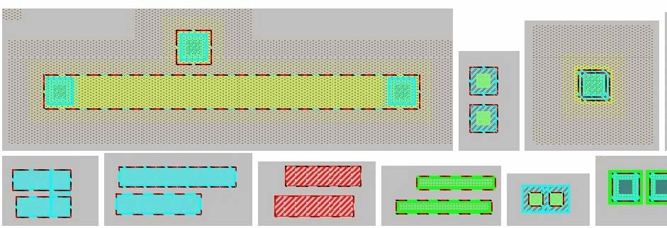
It looks like the techfile is addressing most of the DRC rules already. There is a need for
spacing rules. But to generate minimum size DRC error rules, a node needs to be deliberate
resized. A way to fail a surround rule has yet to be found.
DRC error 1 Spacing ( 'Via1') Metal-1-Metal-2-Con['contact@10'] LESS (BY 2) THAN 3 TO Metal-1-Metal-2-Con['contact@9'] [rule '8.2 Mosis']
DRC error 3 Spacing ( 'Metal-1') Metal-1-N-Active-Con['contact@8'] OVERLAPS (BY 7.5) Metal-1-N-Active-Con['contact@7'] [rule '7.4 Mosis']
DRC error 5 Minimum size error on X axis cell 'a{lay}' Metal-1-N-Active-Con['contact@6'] LESS THAN 4 IN SIZE (IS 5) [rule '6.2, 7.3']
DRC error 6 Spacing ( 'Metal-1') Metal-1-Polysilicon-1-Con['contact@0'] LESS (BY 2.5) THAN 4 TO Metal-1-Polysilicon-1-Con['contact@1'] [rule '7.4 Mosis']
DRC error 7 Spacing ( 'N-Active') N-Active-Resistor['resnactive@0'] LESS (BY 1.5) THAN 3 TO Metal-1-N-Active-Con['contact@2'][rule '2.4 Mosis']
DRC error 9 Spacing ( 'Metal-1') Metal-1-Metal-2-Con['contact@5'] LESS (BY 2.5) THAN 4 TO Metal-1-Metal-2-Con['contact@4'] [rule '7.4 Mosis']
DRC error 13 Notch ( 'Metal-1') arc Metal-1['net@8'] LESS (BY 3) THAN 4 TO arc Metal-1['net@10'] [rule '7.4 Mosis']
DRC error 15 Spacing ( 'Metal-1') arc Metal-1['net@0'] LESS (BY 3) THAN 4 TO arc Metal-1['net@1'] [rule '7.4 Mosis']
DRC error 17 Spacing ( 'Metal-2') arc Metal-2['net@3'] LESS (BY 2.5) THAN 4 TO arc Metal-2['net@4'] [rule '7.5 Mosis']
DRC error 19 Spacing ( 'Polysilicon-1') arc Polysilicon-1['net@5'] LESS (BY 2.5) THAN 4 TO arc Polysilicon-1['net@6'] [rule '7.0 Mosis']

DRC error 12 Minimum width/height error((X axis)) cell 'a{lay}' N-Active-Node['plnode@3'], layer 'N-Active' LESS THAN 3 WIDE (IS 2) [rule '2.1 Mosis']
The results of various DRC experiments are shown above.
==========================CONCLUSIONS==============================
It looks like ELECTRIC should be able to produce production worthy Integrated Circuits.
There are a few areas where some attention is needed.
First off, everything is done in terms of layout units. Care needs to be taken
that the translations to both layout and schematic are done right.
Second, matching of schematic to layout is also only done in layout units. As per
the schematic. It is not very hard to write a web page calculator to convert layout
units to resistance values. The schematic does attempt to be translated to the
correct spice format as far as widths and lengths and resistance values. Since the
schematic is saved in text format, it would not be hard to write a python
program to read and verify that the layout dimensions and resistance values are all right.
Third, it looks like most DRC rules are being included in the techfile. It looks
like writing the techfile well is going to be the main area where spending some
time will save a lot of time.
Forth, layout in ELECTRIC is being done exactly like schematic entry. All design
engineers know how to do schematic entry. For Mixed Signal Integrated Circuits,
the structure of the signal path seems to pull the layout to be done very close
to the schematic anyway. So does this mean design engineers could layout a circuit
as easily as entering a schematic?